Book Appointment Now

Inside a 6-layer optical module PCB: layer assignment, 100 and 90 ohm targets, Tg 180 material, the split ENIG plus hard gold finish and where yield is lost.
6-Layer Optical Module PCB: Stackup, Impedance and Finish
A 6-layer optical module PCB carries the conversion that defines the whole product: electrical in, light out, and back again. Every signal that enters the module at 25G, 100G or 400G passes through this board twice, so the stackup has to give the DSP, driver and TIA a quiet reference, a low impedance power path and a controlled 50 or 100 ohm environment without adding insertion loss of its own. This guide is written for the engineer or buyer who has to release that board: which layer does what, why six layers became the default above 25G, what the impedance tolerance actually buys, how the material choice behaves at temperature, why the finish is split between ENIG and hard gold, and which of the cost drivers can be moved without touching signal integrity. The parameters quoted here are the values we build against, not catalogue ranges.
Table of Contents
- What a 6-Layer Optical Module PCB Has to Do
- Why Six Layers Become the Default Above 25G
- Layer Assignment and Stackup on a 6-Layer Optical Module PCB
- Impedance Targets and What the Tolerance Really Buys
- Material Selection: Tg 180 FR-4 Grade and Its Limits
- Split Surface Finish: ENIG in the SMT Area, Hard Gold on the Fingers
- Process Control Points That Decide Yield
- Four, Six or Eight Layers: A Selection Table
- What to Ask Before You Release the Stackup
- What Drives Cost on a 6-Layer Optical Module PCB
- FAQ
- Get the Stackup Reviewed Against Your Channel Budget
What a 6-Layer Optical Module PCB Has to Do
The board sits between a host connector on one edge and an optical subassembly on the other. In between are a DSP or CDR, a laser driver, a transimpedance amplifier and a dense field of decoupling. Its job is to move a differential pair from the host fingers to the driver with as little reflection and loss as the channel budget allows, while keeping a multi-ampere burst current off the same reference the pair is using.
That combination is what separates an optical module board from a generic six layer digital board. The signal environment is narrowband and very fast, the power environment is bursty, and the mechanical environment includes repeated insertion into a cage. Each of those pushes the stackup in a different direction, and a 6-layer optical module PCB is the point where all three are still satisfied at a cost the market accepts.
It also has to survive being handled. Module boards are small, thin relative to their length, and usually panelised ten up with the fingers on the panel edge. Everything from panel design to routing of the fingers affects whether the finished module inserts cleanly on the tenth thousandth cycle.
Why Six Layers Become the Default Above 25G
A four layer board can carry 10G traffic and often does. Above 25G the numbers stop cooperating: with only two inner layers you can have ground or power, not both, and the layer that loses becomes the one your return current has to borrow. Borrowed return paths create the impedance discontinuities that show up as eye closure after the module is assembled and cannot be reproduced on a coupon.
Six layers solves that by giving two complete ground planes and one dedicated power plane. High speed pairs reference L2 from above and L5 from below, so a via transition crosses from one reference to another that is at the same potential, which is the whole point of the plane pair. The two grounds are stitched around the via field so the return current never has to detour across the board.
The cost step from four to six layers is real but modest compared with the rest of a module bill of materials, and it buys margin that no amount of layout tuning recovers on four layers. Eight layers becomes attractive only when the design needs two full routing layers per side, or when the module also carries a dense BGA that forces escape routing through blind vias.
Layer Assignment and Stackup on a 6-Layer Optical Module PCB
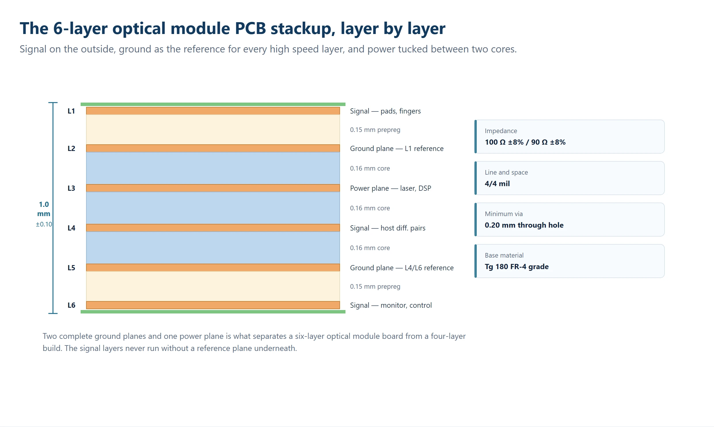
The stackup below is a 1.0 mm build with 35 µm copper on every layer, which is the configuration we quote for most 25G and 100G designs. The dielectric sequence is chosen so that the two high speed signal layers see the same prepreg thickness, because asymmetric dielectric means asymmetric impedance and a pair that behaves differently depending on which side it is routed.
| Layer | Function | Copper | Dielectric to next layer |
|---|---|---|---|
| L1 | Signal, SMT pads, edge fingers | 35 µm | 0.15 mm prepreg (2 × 1080) |
| L2 | Ground plane, reference for L1 | 35 µm | 0.16 mm core |
| L3 | Power plane, laser and DSP rails | 35 µm | 0.16 mm core |
| L4 | Signal, host side differential pairs | 35 µm | 0.16 mm core |
| L5 | Ground plane, reference for L4 and L6 | 35 µm | 0.15 mm prepreg (2 × 1080) |
| L6 | Signal, monitor and control | 35 µm | Finished board 1.0 ±0.10 mm |
Two details matter more than the table. First, keep L1 and L6 copper balanced; an unbalanced pair of outer layers is the most common cause of bow after reflow on a long thin module board, and bow changes the finger height in the cage. Second, do not route high speed pairs on L4 in the same direction as L1 for any distance. Cross the routing at right angles where the two layers overlap, so broadside coupling between them stays negligible.
Impedance Targets and What the Tolerance Really Buys
Optical module interfaces are standardised at the connector, so the targets are not negotiable. What is negotiable is the tolerance you specify, and that is where cost and yield diverge. The table below shows the targets we hold and the classes available around them.
| Interface or signal | Target | Tolerance class | Where it applies |
|---|---|---|---|
| SFP, SFP+ host pair | 100 Ω differential | ±8% | Fingers to DSP |
| QSFP28, QSFP-DD host pair | 90 Ω differential | ±8% | Fingers to DSP and CDR |
| Single ended control and monitor | 50 Ω | ±10% | I2C, reset, status |
| Tight tolerance option | as target | ±10% standard, ±8% on request, ±5% by review | Whole board or selected nets |
| Test method | TDR on a coupon | Coupon per panel | Reported with the lot |
±8% is the working class for 100G designs and it is not marketing. On a 100 Ω pair, ±8% is 8 Ω of window; the reflection coefficient at the worst case is small enough that the link budget still closes after the connector and the optical subassembly are counted. Tightening to ±5% is possible by review, but it changes etch compensation, prepreg selection and the amount of test coverage, so it should be asked for on specific nets rather than board wide.
The mechanism that holds the tolerance is boring and worth stating explicitly: stackup designed first, trace width compensated for etch, then impedance measured on a coupon by TDR from the same panel. A fabricator that quotes a tolerance without a coupon requirement is quoting a hope. The impedance measurement guide explains how coupon design and TDR setup change the number you get back.
Material Selection: Tg 180 FR-4 Grade and Its Limits
The default material for this board is a Tg 180 FR-4 grade laminate, 0.5 oz to 1 oz copper with a dissipation factor in the 0.002 to 0.004 range at 1 GHz depending on grade. It holds dimensional stability through the reflow profile, keeps Dk predictable over the module operating range and survives the thermal cycling that comes with being plugged in and out of a cage.
| Material class | Tg | Where it fits | Trade off |
|---|---|---|---|
| S1000-2M | 180 °C | Default for 25G and 100G modules | Higher lamination temperature, higher cost than Tg 150 |
| S1170G | 170 °C | Cost sensitive 10G to 25G designs | Less margin at the top of the reflow window |
| S1150G, halogen free | ≥150 °C | Projects with a halogen restriction | Different Dk, re-qualify the stackup |
| S1000H, mid-Tg | 150 °C | Short life consumer modules | Less dimensional stability through reflow |
Two practical notes. Material name alone does not set impedance; the same grade from two suppliers can differ by enough in Dk to move a 100 Ω pair outside ±8%, so the stackup is qualified against the specific laminate rather than the grade. And if a halogen-free requirement lands mid-project, treat it as a stackup change rather than a material substitution, because Dk and thickness tolerances move together. The laminate selection guide covers the comparison in more detail.
Split Surface Finish: ENIG in the SMT Area, Hard Gold on the Fingers
An optical module board has two surfaces with opposite requirements. The SMT area needs a flat, solderable pad for fine pitch packages. The fingers need a hard, wear resistant contact that survives thousands of insertion cycles. No single finish does both well, which is why the board carries two.
| Area | Finish | Thickness | Why |
|---|---|---|---|
| SMT pads | ENIG | 2 µin gold over 3–5 µm nickel | Flat and coplanar for QFN and BGA lands, good wetting |
| Edge fingers | Electrolytic hard gold | 30 µin | Hardness and wear resistance for repeated insertion |
| Finger bevel | Rout bevel | 30° or 45° | Lowers insertion force, protects the contact edge |
| Board thickness | Finished | 1.0 mm (0.6–2.0 mm range) | Sets finger height in the cage |
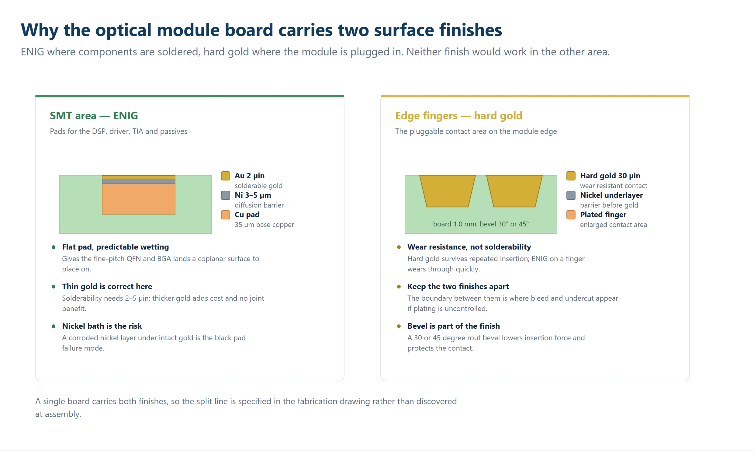
The boundary between the two finishes is the part that gets neglected. Plating resist has to stop exactly where the gold stops, or you get gold bleed into the solderable area and undercut at the finger shoulder. Both defects pass visual inspection and fail at assembly or at the twentieth insertion. Specify the boundary dimension on the fabrication drawing rather than relying on the fabricator’s default.
Process Control Points That Decide Yield
On this board the yield risk is concentrated in six places, and each of them is measurable. Asking a fabricator which of these they record, and what the last month looked like, tells you more than a capability brochure. Design data arrives as Gerber data plus a drill file, so confirm that layer naming matches the stackup before anything is tooled.
- Etch compensation on the 4/4 mil layers, verified by first article line width measurement rather than by eye
- Lamination thickness after press, because a 0.02 mm shift in dielectric moves a 100 Ω pair by roughly 3 Ω
- Drill quality at 0.20 mm with controlled tool life, checked by hole wall inspection before plating
- Plating thickness in the barrel, targeted at 20 µm or more with a cross section on the first article
- Solder mask registration to ±0.05 mm so the dam between fine pitch pads survives
- Finger bevel geometry and gold thickness measured after bevel, since bevel exposes the plated edge
The last item catches teams out. Gold is measured on the flat of the finger, but the bevel cuts through the plated edge and exposes whatever the plating actually deposited. If the bevel is routed after plating without a check, the contact that matters most, the one that touches the cage spring, is the one nobody measured.
Four, Six or Eight Layers: A Selection Table
Most sourcing decisions on this product come down to one question: is the design already committed to 25G and above, or is it a lower rate module where cost dominates. The table is a starting point, and the real answer comes from the channel budget.
| Build | Typical rate | Relative cost | When it is the right answer |
|---|---|---|---|
| 4 layers, 1.0 mm | Up to 10G | 1.0 baseline | Cost driven modules with a short host trace and no CDR |
| 6 layers, 1.0 mm | 25G to 100G | Roughly 1.25–1.5x baseline | The default for SFP28, QSFP28 and QSFP-DD style designs |
| 8 layers or 6 layer HDI | 100G to 400G | Roughly 1.8–2.5x baseline | Dense BGA escape, multiple supply domains, or long host traces |
| Any-layer HDI | 400G and above | Multiple of the baseline, quoted per design | When via stubs and escape density cannot be solved any other way |
These multipliers are relative planning figures, not prices; the actual number comes from a stackup review with the real panel. What matters at selection stage is that the jump from four to six layers is far cheaper than the jump from six to eight, so if a design is marginal at 25G, spend the small step now rather than re-spinning later. If the design already needs blind vias to escape a DSP, the 2-stage HDI prototype route is usually cheaper than an eight layer through-hole build.
What to Ask Before You Release the Stackup
The questions below are the ones that separate a fabricator who builds optical module boards from one who has the layer count and nothing else. None of them require a factory visit to answer.
- Which laminate grade will you use, and what Dk did you qualify the 100 Ω stackup against
- Can you supply a TDR coupon report from the same panel, and what is the sampling rate per lot
- How do you control the boundary between ENIG and hard gold, and what is the tolerance on that dimension
- What is your measured finger bevel angle and gold thickness after bevel
- What is the finished thickness tolerance, and how is bow controlled on a 10-up panel
- Which acceptance class will you inspect to, and can you name it in the quotation
Naming the acceptance class in the quotation matters more than it sounds on this product, because the pads are small and the fingers are the interface. A class named at order becomes a shared specification; a class assumed becomes an argument after the first lot. The class definitions themselves are published in the IPC standards library, so the number can be quoted exactly rather than paraphrased. The 6-layer optical module PCB product page lists the build envelope we hold for 25G to 400G designs, and the manufacturing capability page covers the surrounding process range.
What Drives Cost on a 6-Layer Optical Module PCB
Cost on this board is dominated by three things: the laminate grade, the surface finish combination and the impedance tolerance class. Layer count and panel size set the floor, but they are fixed early and rarely where the argument happens.
| Driver | Effect on cost | Can it be moved without touching signal integrity |
|---|---|---|
| Laminate grade | Largest single material factor | Yes, if the rate drops to 10G and the stackup is re-qualified |
| Split finish, ENIG plus hard gold | Two plating processes and a boundary control step | No, the fingers need hard gold at any rate |
| Gold thickness on the fingers | Scales with specification | Partially, 30 µin is the working value for repeated insertion |
| Impedance class ±8% versus ±10% | Etch compensation and test coverage | Yes on non-critical nets, no on the host pairs |
| Panel utilisation | Largest geometric factor | Yes, by matching the panel to the module outline and array |
| Test and report package | Coupon, cross section and probe steps | First article only unless the customer requires per lot |
The most common over-specification we see is a board wide ±5% impedance requirement on a design that only needs ±8% on two pairs. The second most common is asking for thicker gold on the fingers than the insertion count justifies. Both push cost up without changing whether the module links. Conversely, the most common under-specification is leaving the finish boundary undefined, which is free to specify and expensive to discover.
Frequently Asked Questions
Why does an optical module PCB need six layers instead of four?
Above 25G the board needs two complete ground planes plus a dedicated power plane. On four layers you can have ground or power on the inner layers but not both, so return current borrows a path and the impedance discontinuities close the eye after assembly. Six layers gives L2 and L5 as references and L3 as power, which is the minimum for a clean via transition.
What impedance tolerance should I specify for a 6-layer optical module PCB?
±8% on the 100 Ω SFP pair and the 90 Ω QSFP pair is the working class, with ±10% acceptable on single ended control nets. ±5% is available by review but should be specified on selected nets, because applying it board wide changes etch compensation and test coverage without improving the link budget.
Which laminate is used for optical module boards?
A Tg 180 FR-4 grade is the default for 25G and 100G designs, with dissipation factor in the 0.002 to 0.004 range at 1 GHz. Tg 170 grades suit cost sensitive lower rate designs, and halogen free grades are available when the project requires them, but each change re-qualifies the impedance stackup.
Why are the edge fingers hard gold instead of ENIG?
Hard gold is specified for wear. A module may be inserted thousands of times, and ENIG on a finger wears through and exposes nickel, which then oxidises and raises contact resistance. The 30 µin hard gold layer on the fingers is paired with ENIG on the SMT area because solderability and wear resistance are different requirements.
What board thickness is standard for an optical module PCB?
Around 1.0 mm finished, with the range typically 0.6 mm to 2.0 mm depending on the cage and the module outline. Thickness sets the finger height in the cage, so the tolerance of ±0.10 mm matters as much as the nominal value, and bow has to be controlled across a ten up panel.
How is a 6-layer optical module PCB tested?
Electrical test is 100 percent flying probe or bed of nails, with a TDR coupon measured per panel to confirm impedance. The coupon is built on the same panel as the product, so what is measured reflects the actual dielectric and etch. First article adds a cross section for hole copper and surface copper.
What drives the cost of a 6-layer optical module PCB?
Laminate grade, the split ENIG plus hard gold finish and the impedance tolerance class are the three biggest factors, followed by panel utilisation and the test and report package. Layer count sets the floor but rarely varies, and moving from four to six layers costs far less than moving from six to eight.
Get the Stackup Reviewed Against Your Channel Budget
Send the layer assignment, the target impedance and the rate you are designing for, and the review comes back with a stackup, a coupon plan and the finish boundary drawn on the fabrication notes.
The PCB manufacturing services overview covers what the review includes, from DFM through first article.