Book Appointment Now

What substrate-like PCB (SLP) is, how the mSAP process reaches 25/25 um lines and spaces, and a decision table for choosing SLP over standard HDI.
Substrate-Like PCB (SLP): mSAP Process, L/S Limits and Uses
When a flagship smartphone mainboard, a wireless module or a fitness wearable runs out of routing space, the usual answer – adding another HDI stage – stops paying off. Wiring density no longer improves much with conventional subtractive etching, yet the industrial design still demands a thinner board carrying more components in the same footprint. This is exactly the gap that the substrate-like PCB (SLP) was developed to close: a rigid circuit board that borrows manufacturing processes from IC packaging substrates while remaining, functionally, a component-carrying PCB.
This guide explains what a substrate-like PCB actually is, how the mSAP process reaches 25/25 um line and space, where SLP sits between standard HDI and true IC substrates, and – most practically – a decision table for when moving from HDI to SLP is justified and when it is not. All values cited are typical industry figures; exact capability for a specific stackup is confirmed at engineering review.
Table of Contents
- What Is a Substrate-Like PCB (SLP)?
- SLP vs HDI vs IC Substrate: Where the Line Falls
- How the mSAP Process Builds 25 um Lines
- Line/Space and Thickness: What Each Process Step Buys
- Why SiP Designs Drive SLP Adoption
- Where Substrate-Like PCB Is Used Today
- Designing for SLP: Materials, Vias and Density Trade-offs
- Manufacturing Requirements That Make or Break SLP Yield
- SLP vs HDI: a Cost-Logic Decision Table
- FAQ
- Get Your SLP Stackup Reviewed Before You Commit
What Is a Substrate-Like PCB (SLP)?
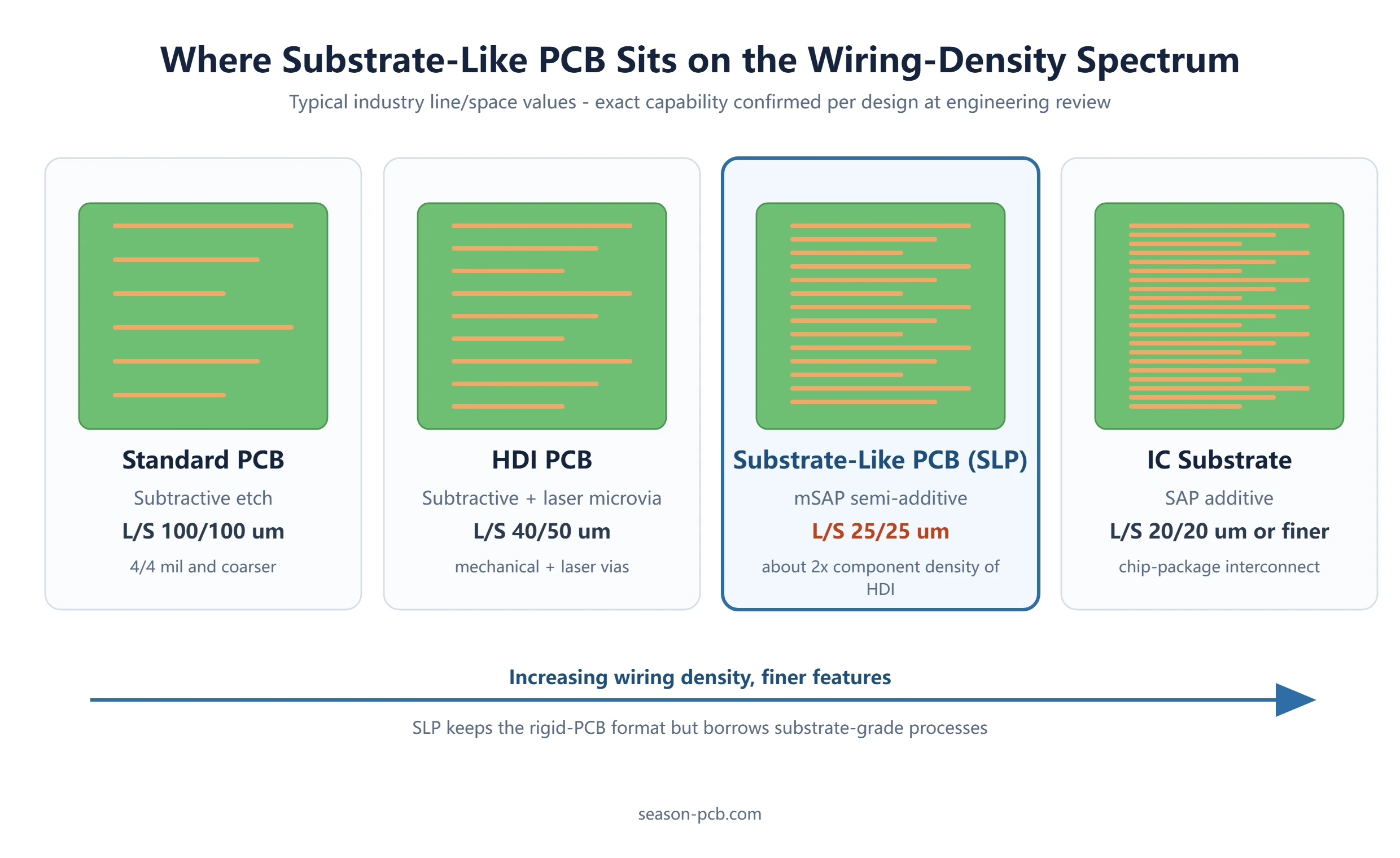
A substrate-like PCB is a rigid printed circuit board whose wiring precision approaches that of a semiconductor package substrate. Where a conventional HDI board is etched with subtractive chemistry down to roughly 40/50 um line and space (L/S), an SLP is formed with a modified semi-additive process (mSAP) that reliably produces L/S around 25/25 um and below 30 um minimum lines.
The defining characteristic is that the SLP has not crossed into packaging territory. Its job remains the same as any circuit board: to carry and interconnect active and passive components – application processors, memory, RF front ends, power management ICs. Because it still mounts components rather than bonding bare die, it keeps the rigid-PCB format, standard assembly flows and connector interfaces. The name says it plainly: a PCB that behaves like a substrate.
The practical payoff is density. In the same board area, an SLP mainboard can carry roughly twice the component count of a comparable HDI build, which is why flagship smartphone mainboards adopted the technology and why wearables and compact modules followed.
SLP vs HDI vs IC Substrate: Where the Line Falls
The three board families blur into each other, so it helps to compare them on process, geometry and role rather than on marketing labels. If you need a refresher on how conventional builds differ first, see our HDI vs standard PCB comparison.
| Attribute | Standard HDI PCB | Substrate-Like PCB (SLP) | IC Substrate |
|---|---|---|---|
| Pattern process | Subtractive etching | mSAP (semi-additive) | SAP (fully additive) |
| Typical L/S | 40/50 um and coarser | 25/25 um, below 30 um min line | 20/20 um or finer |
| Typical microvia | Laser, about 0.10 mm | Laser, smaller pitch stacks | Laser, finest pitch |
| What it carries | Components | Components, highest density | Bare die / chip package |
| Typical role | General electronics mainboards | Smartphone-class mainboards, modules | Chip packaging interconnect |
| Assembly | Standard SMT | Standard SMT, fine-pitch | Die-attach, wire/bond or flip-chip |
Two boundaries matter for sourcing decisions. First, SLP remains in the PCB category: it accepts packaged components and standard assembly, so your CM flow barely changes. Second, the process jump from HDI to SLP is not incremental – it replaces the etching step that defines HDI, which is why cost and supplier capability questions should be asked before the layout is frozen.
How the mSAP Process Builds 25 um Lines
Subtractive etching has a physical ceiling. When acid eats away unwanted copper it attacks sideways as well as downward, so as target traces shrink, the etched walls become trapezoidal and line width loses control. Below roughly 30 um, yield collapses. The outer-layer patterning step that works for standard boards simply cannot reach substrate-class geometry.
mSAP inverts the logic. Instead of etching copper away, it plates copper only where traces belong:
- Start with an ultra-thin seed copper foil laminated to the dielectric.
- Laminate and expose a fine-line photoresist mask defining the traces.
- Electrolytically plate copper up to full thickness only inside the mask openings.
- Strip the resist, then flash-etch the seed foil – a lateral cut of only a micrometre or two, not a full-thickness etch.
- Repeat per build-up layer, pairing with laser microvias.
Because the final etch removes only the thin seed layer, line shape stays rectangular and width holds at 25 um and below. Fully additive SAP pushes the same idea further – plating onto bare dielectric with no seed foil at all – and is the standard route for IC substrates at 20/20 um and finer. The progression from subtractive to mSAP to SAP is therefore not about preference; each step buys a geometry the previous one cannot hold.
Line/Space and Thickness: What Each Process Step Buys
The table below summarizes a typical industry progression for smartphone-class mainboards. Note the counter-intuitive middle row: mSAP boards are not always thinner, because layer count and rigidity targets also drive thickness.
| Process generation | Typical L/S | Layer count | Board thickness |
|---|---|---|---|
| Subtractive (HDI class) | 40/40 um | 10 layers | 0.65 mm |
| Subtractive, fine-line | 30/40 um | 10 layers | 0.55 mm |
| mSAP (SLP class) | 25/25 um | 10 layers | 0.60 mm |
| SAP (substrate class) | 20/20 um | 8 layers | 0.35 mm |
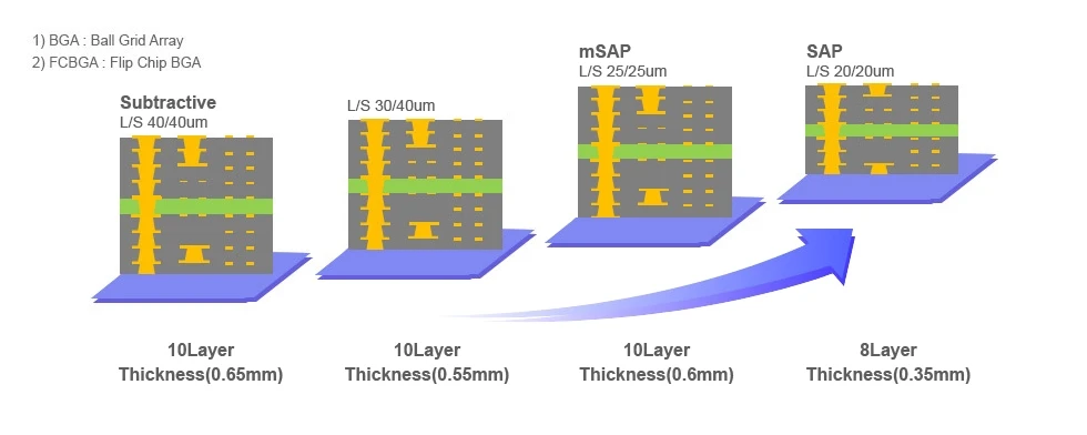
Read the progression as a trade: each move to the right buys finer geometry and, at the SAP end, a dramatic thickness reduction, but it also adds process steps, tightens the supplier base and raises cost. Specifying 20/20 um SAP geometry for a design that routes happily at 40/40 um HDI is paying for capability the layout never uses.
Why SiP Designs Drive SLP Adoption
System-level integration is following two routes. SoC integration merges more functions into one die, but as semiconductor process nodes advance, shrinking digital logic is getting harder and more expensive, and analog, RF and memory functions resist the same node moves. SiP – system-in-package – takes the other route: multiple known-good dies and passives assembled into one package module.
A SiP module with its dense internal wiring needs a carrier whose routing density approaches the substrate class, yet the module itself still mounts onto a system board with standard assembly. That is precisely the SLP envelope: dense enough to host SiP-class interconnect and module fanout, while remaining a PCB in format and flow. As SiP content grows in wearables, RF modules and edge AI devices, demand for substrate-like PCB follows.
Where Substrate-Like PCB Is Used Today
The common thread across SLP applications is a constrained enclosure combined with high integration – the point where adding HDI stages stops buying meaningful density. The leading adopters:
- Flagship smartphone mainboards – the original driver, roughly doubling component density per board area versus HDI.
- Wearables – smartwatch and hearable boards where every tenth of a millimetre of thickness and every square millimetre of area is contested.
- Wireless and RF modules – dense fanout around front-end ICs and antennas, often as SiP carriers.
- Camera and sensor modules – fine-pitch image processing ICs in tightly bounded footprints.
- Automotive electronics – compact ADAS camera and radar modules that inherit smartphone-class integration; see our automotive PCB reliability guide.
Note what is not on the list: large consumer boards, industrial controllers and power electronics. When board area is not the binding constraint, SLP economics rarely close, and HDI remains the rational choice.
Designing for SLP: Materials, Vias and Density Trade-offs
Fine geometry changes every downstream decision. Impedance control tightens because a 25 um line tolerates less etch and registration variation – our standard ±10% single-ended and ±8%/±5% differential tolerance windows should be stated on the stackup, not discovered later. Dielectric selection moves toward mid-loss and low-loss laminates to keep insertion loss acceptable at mmWave and multi-gigabit speeds; the PCB materials guide covers the laminate ladder in detail. Laminate systems should come from UL-recognized material listings, for example via UL Solutions.
Via strategy matters as much as traces. Microvia pitch shrinks with the lines, stacked and staggered via chains multiply, and via-in-pad with fill becomes common to survive routing escapes under fine-pitch BGA fanout. Designers moving from HDI should re-examine any-layer HDI interconnect concepts, because SLP build-ups are conceptually their extension. IPC-2226 microvia design rules remain the reference framework here – see the IPC standards library.
Be honest about the capability boundary. A shop running conventional subtractive HDI at 2/2 mil cannot simply accept a 25 um SLP job; mSAP needs dedicated plating chemistry, fine-line imaging and registration systems. Confirm the process route with your fabricator before the stackup is locked, the same way you would confirm any prototype requirement.
Manufacturing Requirements That Make or Break SLP Yield
The yield levers differ from standard PCB production. Line-width control depends on imaging resolution and plating uniformity across the panel, so automated optical inspection shifts from final-article checking to in-process monitoring of plated line geometry. Layer-to-layer registration tightens because a misalignment that a 100 um line would shrug off visibly skews a 25 um one – the same discipline discussed in our layer registration accuracy guide.
Thin cores and build-up films demand gentler handling: thinner materials warp and wrinkle more easily through lamination and desmear, and thin copper layers give etching less margin. First-article cross-sections are effectively mandatory, checking line shape, via fill and interconnect quality layer by layer. None of this is exotic – it is substrate-class discipline applied to a PCB – but it is the reason SLP capacity concentrates in factories that already run IC-substrate or advanced-HDI processes.
SLP vs HDI: a Cost-Logic Decision Table
Absolute pricing varies with stackup, volume and region, so the useful framing is relative cost logic: what actually drives the premium, and which design facts justify paying it. A substrate-like PCB typically sits clearly above a comparable 3-stage HDI build, driven by mSAP plating cycles, fine-line imaging yield and tighter registration overhead.
| Decision factor | Stay with HDI | Move to substrate-like PCB |
|---|---|---|
| Routing congestion | Escapes close with 40/50 um L/S | Fanout fails at HDI geometry or needs unjustified layers |
| Board area budget | Enclosure tolerates current size | Industrial design demands a smaller footprint |
| Layer count trend | Density recoverable by adding 1-2 layers | Layer count escalating faster than area saved |
| Component density | Standard-pitch parts dominate | Fine-pitch SiP, PoP and dense BGA fanout dominate |
| Volume | Prototype or early builds | Stable, high-volume production amortizes process cost |
| Supply chain | Standard HDI supplier adequate | Fabricator must run mSAP or substrate-class processes |
A useful screening exercise: count the net routing channels your densest region needs, then compare against HDI escape capacity. If the deficit survives adding two layers and a finer BGA escape pattern, SLP has a functional case; if not, the premium buys nothing measurable. Our 12-layer 1-stage HDI core board shows where advanced HDI currently tops out for carrier-class builds. For packaging-side alternatives, compare semiconductor package substrates and the BT substrate option.
Frequently Asked Questions
What is a substrate-like PCB?
A substrate-like PCB (SLP) is a rigid circuit board manufactured with semiconductor-substrate processes, most commonly the mSAP semi-additive process, reaching line/space around 25/25 um. It still carries packaged components with standard SMT assembly, so it belongs to the PCB category rather than IC packaging, while offering substrate-class wiring density.
How is SLP different from standard HDI?
HDI boards pattern layers by subtractive etching and typically reach 40/50 um line and space. SLP replaces etching with mSAP plating, holding 25/25 um and below 30 um minimum lines, which roughly doubles routable density per area. The process change is the root difference; everything else – density, via pitch, cost – follows from it.
What is the mSAP process?
Modified semi-additive process: a thin seed copper foil is laminated, a photoresist defines the traces, copper is plated to full thickness only in the pattern, then the seed foil is flash-etched. Because the etch removes only one or two micrometres laterally, line walls stay vertical and width stays controlled at fine geometry – unlike subtractive etching, which attacks sideways and loses control below about 30 um.
What line widths can substrate-like PCB achieve?
Typical SLP production runs at 25/25 um line and space, with minimum lines below 30 um. Fully additive SAP used for IC substrates reaches 20/20 um or finer. Actual capability varies by fabricator, so confirm the process route and tolerances at engineering review rather than assuming a class label guarantees a number.
Is a substrate-like PCB the same as an IC substrate?
No. An IC substrate interconnects bare die inside a chip package using SAP processes at 20 um and finer geometry. An SLP carries packaged components on a system board, keeping standard SMT assembly. SLP sits between HDI and IC substrates: substrate-class wiring precision with PCB-format assembly.
Which products use substrate-like PCBs?
Flagship smartphone mainboards were the first large-scale adopters, followed by smartwatches and other wearables, wireless and RF modules, camera and sensor modules, and compact automotive ADAS modules. The pattern is a space-constrained, high-integration product where adding HDI stages no longer buys meaningful density.
How much more does an SLP cost than HDI?
Expect a clear premium over a comparable 3-stage HDI build, driven by mSAP plating cycles, fine-line imaging yield and tighter registration control; the multiple depends on stackup, layer count and volume. Treat it as a relative-cost decision: if routing congestion and board-area budget genuinely require 25 um geometry, the premium is justified – otherwise it is wasted. Final pricing is confirmed at quotation.
Get Your SLP Stackup Reviewed Before You Commit
Deciding between an additional HDI stage and a substrate-like PCB build is a stackup-level decision, and it is cheapest to make before layout freeze. Send us your Gerber data, netlist requirements and target L/S – our engineering team will review the routing density, via strategy and material selection, and confirm whether mSAP-class processing is actually required for your design.
Season Multilayer Circuit manufactures 2-30 layer rigid PCBs from prototype through volume production as part of the 998 PCB Group, with 3,000,000 m2 of annual group capacity across three manufacturing sites. For an overview of our advanced interconnect capability, start with the HDI PCB technology guide or our PCB manufacturing services.