Book Appointment Now

PCB backdrilling removes the via stub that hurts high-speed signals. Learn when to specify backdrill, how depth control works and what it costs.
PCB Backdrilling Explained: Via Stub Removal for Signal Integrity
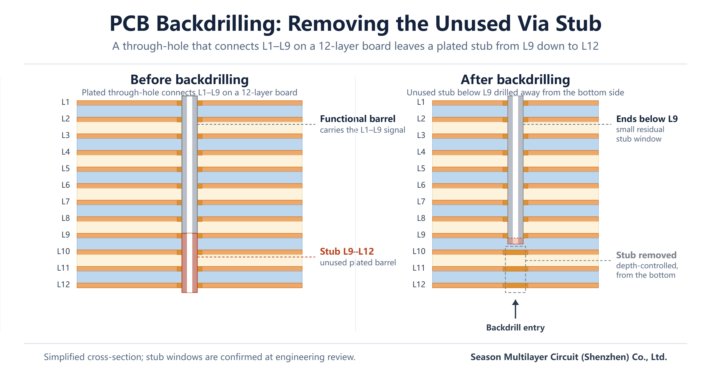
A plated through-hole is the simplest way to connect two layers of a PCB, but on a thick high-speed board it is rarely innocent. If your signal enters at L1 and must reach L9 of a 12-layer board, the barrel keeps going — down through L10, L11 and L12 — leaving a section of unused plated copper hanging below the last connected layer. That unused section is the via stub, and at multi-gigabit speeds it behaves like an unmatched antenna attached to your net. PCB backdrilling is the controlled-depth drilling step that removes it.
This guide explains what backdrilling actually removes, why stub length matters for signal integrity, when the process is worth specifying and when it is not, how factories control drill depth, and what the extra process step means for cost and lead time. The goal is that you can look at your own stackup and make a defensible backdrill decision before you request a quote — not after a signal-integrity lab report tells you the eye diagram is collapsed.
Table of Contents
- What Is PCB Backdrilling?
- Why Via Stubs Damage High-Speed Signals
- When to Specify PCB Backdrilling (and When to Skip It)
- The Backdrilling Process, Step by Step
- Depth Control and the Residual Stub Window
- Backdrilling vs Adding Blind and Buried Vias
- Quality Checks for Backdrilled Boards
- Where Backdrilled PCBs Are Used
- What Backdrilling Adds to Cost and Lead Time
- Design Checklist Before You Order a Backdrilled Board
- FAQ
- Get Your Stackup Reviewed for Backdrill Feasibility
What Is PCB Backdrilling?
PCB backdrilling (also called controlled-depth drilling or stub removal) is a secondary drilling operation performed on a multilayer board after the through-holes have been drilled and plated. The drill enters from the back side of the board and removes the portion of the plated barrel that extends below the last layer the net actually uses. What remains is a functional barrel connecting only the signal layers, plus a small, deliberately tolerated remainder called the residual stub.
The key word is controlled depth. The backdrill does not simply cut the board in half; it stops at a defined depth derived from the dielectric thickness between the target layer and the layer below it. A 12-layer backplane might carry hundreds of through-hole vias that connect L1 to L9, while the physical hole runs from surface to surface. Backdrilling converts each of those holes from a 12-layer barrel into an effective 9-layer connection — without changing the layer stackup or re-routing the design.
It helps to be precise about what is and is not removed. The drill removes plated copper and hole wall, not active circuitry. Pads on the layers below the stop depth are generally left intact unless the design specifies pad removal, and the lamination structure of the board is untouched. For a visual walk-through of how this fits into the wider manufacturing sequence, see our PCB drilling process overview.
Why Via Stubs Damage High-Speed Signals
An unused stub is an open-circuited transmission line hanging off the middle of your signal path. Energy travelling down the barrel splits at the junction: part of it continues to the receiving layer, and part of it runs down the stub, hits the open end, and reflects back. That reflected energy arrives back at the junction delayed and out of phase, where it interferes with the wanted signal as ripple on the eye diagram, increased jitter and degraded insertion loss.
The damage is frequency-dependent. A stub behaves like a quarter-wave resonator: at the frequency where the stub length corresponds to a quarter of the signal wavelength in the dielectric, the reflections add coherently and produce a sharp notch in the insertion loss profile. The resonance frequency is inversely proportional to stub length — approximately f = c / (2 · √Dk · L), where L is the stub length and Dk the dielectric constant. As data rates rise, the operating frequency climbs toward that notch, which is why a via that is perfectly acceptable on a 125 MHz board can be fatal on a 25 Gbps serial link.
The practical consequence shows up in channel margin. Longer stubs pull the resonance notch down into the operating band and steepen the loss slope around it, closing the eye at the receiver. Removing the stub pushes the notch far above the Nyquist frequency, where it can be ignored. This is the entire value proposition of backdrilling: it does not make the via better in any way except deleting the part that reflects.
When to Specify PCB Backdrilling (and When to Skip It)
Backdrilling is not free — it adds a drilling pass, a depth-control requirement and inspection effort — so the decision should be driven by stub length against edge rate, not by habit. The two variables that matter most are how thick the board is below the last used layer, and how fast the net switches. A 1.6 mm four-layer board with 100 Ω single-ended traces rarely justifies the process; a 2.4 mm, 12-layer backplane carrying multi-gigabit links almost always does.
| Design scenario | Typical build | Backdrill recommendation |
|---|---|---|
| Low-speed control signals, board under 1.6 mm | 2–4 layers, through-hole only | Not needed — stub effect is negligible |
| Mixed-signal board, nets up to a few Gbps, short remaining stub | 6–8 layers | Evaluate per net; often skippable |
| Multi-gigabit serial links on a thick board | 10–14 layers, high-speed laminate | Recommended for the high-speed nets |
| Backplanes, midplanes, server and switch cards | 12+ layers, press-fit connectors | Standard practice — specify it in the fab notes |
| Cost-driven consumer board with room to re-route | 4–6 layers | Skip; move critical nets to outer layers instead |
A useful screening rule: estimate the stub length from your stackup (the distance from the last used layer to the bottom surface) and compare it with the signal’s rise-time length. If the stub is electrically short — roughly under a tenth of the distance the edge travels during its rise time — the reflection is usually tolerable. If it approaches a quarter of that length or more, plan for backdrilling or for a blind/buried via structure. Our high-speed PCB design rules guide covers this budgeting in the context of a full stackup review.
Note the alternative hiding in that last row: re-routing. If only a handful of nets are high speed, moving them to outer layers (which need no stub) can be cheaper than adding a process step. Backdrilling wins when many layers of routing sit between the connector and the transceiver, which is exactly the geometry of backplanes and server boards.
The Backdrilling Process, Step by Step
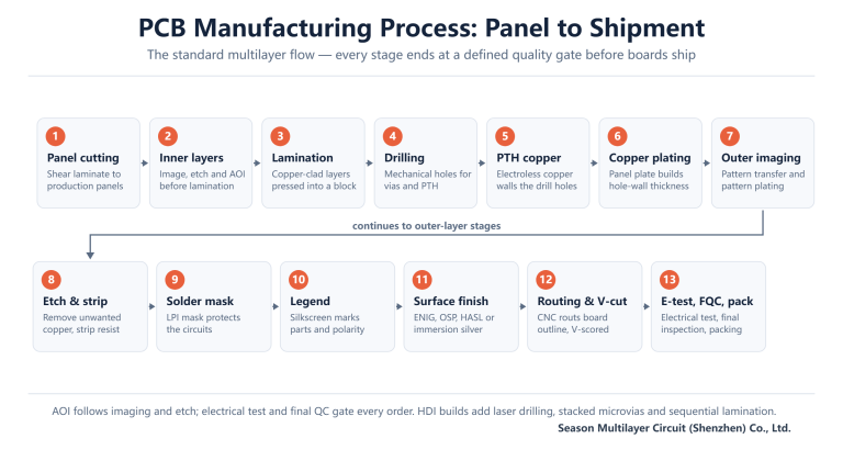
Backdrilling is woven into the normal multilayer flow rather than bolted on at the end, because the backdrill machine re-uses the pilot positions of the first drilling pass. The sequence below reflects how a backdrilled build moves through a production floor.
| Step | What happens | Why it matters |
|---|---|---|
| 1. First drill + pilot holes | Tooling and pilot holes are drilled; through-holes are drilled at registered positions | The pilot holes become the positional reference for the backdrill pass |
| 2. Dry-film seal and plating | Tooling holes are sealed with dry film; the panel is electroless copper plated and then electroplated | Builds the conductive barrel that later becomes the stub to remove |
| 3. Outer layer imaging | Outer circuit pattern is printed, exposed and developed | Defines which pads and traces connect to the barrel |
| 4. Pattern plating | The outer pattern is electroplated to final thickness | Completes the electrical connection through each layer |
| 5. Backdrill pass | The same machine re-registers to the pilot holes and drills from the bottom to the programmed depth | Removes the unused barrel below the last connected layer |
| 6. Rinse and clean | Holes are flushed to remove drill debris | Leftover chips in a backdrilled hole create contamination and reliability risks |
Two details deserve attention. First, registration between the first drill and the backdrill is what keeps the process safe: the backdrill bit must stay inside the original barrel, so the depth window must absorb both drilling tolerance and layer-to-layer thickness variation. Second, the backdrill bit is slightly larger than the original drill — it must cleanly cut the plated wall rather than slide along it. Both points are why the process belongs on qualified equipment rather than as an improvised second setup.
Depth Control and the Residual Stub Window
Modern backdrill machines do not trust a blind depth count. As the spindle approaches the panel, a sensing system detects contact with the surface copper and establishes a true zero reference per hole; the machine then drills to the programmed depth from that reference. This compensation matters because panel thickness varies slightly across the panel, and a depth measured from a nominal surface would silently eat into the tolerance budget.
The designer’s job is to define how deep “deep enough” is. The spec that matters is the residual stub window: the maximum copper height allowed to remain below the last connected layer. Too deep, and the drill encroaches on the dielectric and pads of the layer below the stop target; too shallow, and stub residue erodes the signal-integrity benefit. On qualified production equipment, depth control is held to roughly the ±0.05 mm class; the binding constraint is usually the dielectric thickness tolerance between layers, so the achievable residual stub should be confirmed at engineering review rather than assumed from the drill spec alone.
When you document backdrill in the fab notes, specify it per net class or per drill file rather than as a blanket instruction: which drills get backdrilled, from which side, to which layer reference. Ambiguity here is the most common cause of a quote coming back with exceptions attached. If your stackup is still fluid, our team reviews stub windows as part of a PCB stackup and HDI technology review before the build is released to the floor.
Backdrilling vs Adding Blind and Buried Vias
Backdrilling is not the only way to eliminate a stub — the other classic route is to avoid the full through-hole in the first place. Blind and buried vias connect only the layers they need, so no stub exists to remove. The trade-off is structural: each additional lamination cycle for sequential build-ups adds process steps and yield risk, which is why many backplane designers prefer a plain through-hole plus backdrill over a multi-lamination alternative.
| Approach | Best suited for | Trade-offs |
|---|---|---|
| Through-hole + backdrill | Thick backplanes with many through-vias; press-fit connector fields | Extra drill pass and depth control, but lamination stays simple |
| Blind vias | Outer-layer fanout to the first inner layer | No stub, but one build-up cycle per side |
| Buried vias | Dense inner-layer routing between specific cores | No stub, but sub-board lamination before final press |
| Re-route critical nets on outer layers | Sparse high-speed nets on otherwise simple boards | No special process, but consumes outer-layer routing resources |
For deep dives on the sequential-build alternatives, see our guides to stacked versus staggered HDI vias and the overall HDI PCB technology landscape. In practice, the decision is driven by layer count and via density: the more layers your net must tunnel past, the more attractive backdrilling becomes relative to adding lamination cycles.
Quality Checks for Backdrilled Boards
Because backdrill depth lives inside the board, verification is a mix of process control and sampling. Depth is proven with cross-sections: coupon holes drilled alongside production are sectioned and measured under a microscope to confirm the residual stub sits inside the agreed window and that no connected layer was over-drilled. Registration between the first drill and the backdrill pass is checked on the same coupons.
Electrical verification closes the loop. Time-domain reflectometry on coupon traces reveals the stub as a characteristic impedance dip; on a properly backdrilled board the dip shrinks to a small residual signature. Our impedance measurement guide explains how TDR and VNA methods separate stub effects from ordinary impedance variation. For high-volume builds, the coupon strategy — how many, where they sit on the panel, which nets they model — is agreed as part of the engineering review.
It is also worth knowing what backdrill does not compromise. The mechanical strength of a via is dominated by the barrel section that remains plated through the connected layers, and backdrilled holes on production boards routinely pass thermal cycling and solder-shock expectations for their class. The failure modes to police are process ones: mis-registered backdrills that nick the wrong layer, debris left in holes, and residual stubs that quietly exceed the window.
Where Backdrilled PCBs Are Used
Backdrilling follows high-speed architecture. Communication equipment and data-center infrastructure — switch fabrics, line cards, server backplanes — combine high layer counts with multi-gigabit serial links, making them the natural home of the process. The same logic extends to compute platforms with dense connector breakout, where every via in a differential pair is a potential reflection site.
| Parameter | Example build: 12-layer automotive high-speed backplane |
|---|---|
| Layer count | 12 layers |
| Finished board thickness | 2.4 mm |
| Laminate class | Mid-loss high-speed laminate |
| Board size | 420 × 150 mm (1-up) |
| Outer / inner copper | 1 oz / 1 oz |
| Minimum finished hole | 0.25 mm |
| Trace and space | 5/5 mil |
| Surface finish | ENIG (2 µ″ gold) |
| Special process | Backdrill on high-speed via population |
| Application | Automotive center-console high-speed backplane — the hub linking the vehicle’s electronic systems |
Automotive high-speed domains are a growing share of this demand: central computing platforms and camera-display chains run multi-gigabit links on 8–14 layer boards where stub control directly affects error rates. If your application looks like the table above, our 12-layer automotive high-speed backplane PCB page shows a comparable production build in detail.
What Backdrilling Adds to Cost and Lead Time
In relative terms, backdrilling adds a modest premium over the same board without it: an additional drilling pass with depth control, dedicated program preparation, and coupon-based depth verification. The multiplier grows with hole count and with how tightly the residual stub window is specified, because tighter windows demand slower drilling and more frequent coupon checks. Expect the process to be priced as a special-process adder on the quote — never assume it is covered by the base board price.
Lead time behaves the same way. Backdrill sits between pattern plating and mask, so it lengthens the production chain by one queue position and one inspection gate; for a typical 12+ layer high-speed prototype this is usually absorbed into the standard build window rather than adding a discrete delay, but the exact commitment is confirmed at engineering review once hole counts and depth windows are known.
The counterweight is what it saves. On a backplane-class design, removing stubs can eliminate an entire iteration of signal-integrity debugging — board spins, lab time and schedule slip that cost far more than the process step. Buyers usually get the best outcome by declaring backdrill requirements up front in the fab notes, so the quote reflects one coherent build instead of a revision cycle.
Design Checklist Before You Order a Backdrilled Board
Before releasing a backdrilled build for quote, walk this list. It takes ten minutes and prevents most of the back-and-forth that backdrill RFQs otherwise generate.
- Mark every drill file that requires backdrilling, and from which board side — do not leave it as a text note only.
- Define the residual stub window per net class, derived from your stackup’s dielectric tolerances.
- Check that the layer below each backdrill stop has enough dielectric margin for the drill break-through tolerance.
- Confirm via pad stacks: whether pads on non-connected layers stay or are removed, and how anti-pads are handled.
- Provide a coupon request: which nets to model, where coupons sit, and what depth verification you expect.
- Flag press-fit holes and any via where barrel integrity below the stop layer still matters mechanically.
- State your impedance control requirement (e.g. ±10%, ±8% or ±5%) so coupon testing is scoped correctly.
For context on how backdrill interacts with the rest of a high-speed build, the IPC standards overview at the Global Electronics Association is a good neutral reference point for the design and acceptance standards involved.
Frequently Asked Questions
What is PCB backdrilling?
PCB backdrilling is a controlled-depth drilling step performed after through-hole plating. The drill enters from the back side of the board and removes the unused plated barrel — the stub — below the last layer the net connects, leaving only the functional connection.
Why does an unused via stub cause signal problems?
A stub is an open-ended transmission line attached to the signal path. Energy reflects off its end and returns delayed, interfering with the wanted signal; at the quarter-wave resonance frequency the stub also creates a notch in insertion loss. Longer stubs pull that notch down into the operating band of high-speed links.
When do I actually need backdrilling?
As a rule, when a multi-gigabit net travels through a via that extends well past its last connected layer on a board thicker than about 2 mm. Short stubs on thin boards are usually harmless. Compare stub length with the signal’s rise-time length: if the stub is electrically long, specify backdrill or move the net.
How is backdrill depth controlled?
Machines sense contact with the surface copper to set a true zero, then drill to a programmed depth. The governing spec is the residual stub window — the copper height allowed below the last connected layer. Depth is verified by cross-sectioning coupons from the production panel.
Does backdrilling weaken the via or the board?
The via’s mechanical strength comes from the plated barrel through the connected layers, which backdrilling leaves untouched. Production backdrilled holes routinely pass the thermal and solder-shock expectations of their class. The risks to manage are process ones: mis-registration and debris, both covered by inspection.
Can backdrilling replace blind and buried vias?
Sometimes. Both approaches eliminate stubs, but they trade differently: blind and buried vias avoid the stub at the cost of extra lamination cycles, while backdrill keeps a simple through-hole stackup and adds a drilling pass. On thick backplanes with many through-vias, backdrill is usually the leaner choice.
How much does backdrilling add to cost and lead time?
It is priced as a special-process adder: one more drilling pass, depth program preparation and coupon verification, scaling with hole count and window tightness. Lead time usually absorbs into the standard window for 12+ layer prototypes, but the exact premium and commitment should be confirmed at engineering review.
Get Your Stackup Reviewed for Backdrill Feasibility
If your board carries multi-gigabit nets through a thick stackup, send us the Gerber data and a note on which nets matter. Our engineering team will check stub lengths against your layer stack, propose a residual stub window that survives dielectric tolerances, and confirm the backdrill scope in the quote — before anything reaches the drilling floor.
Submitting early is the cheapest schedule insurance available: one review pass replaces the classic loop of lab-measured failures and a respin. Start with our PCB manufacturing services page and attach your stackup questions to the files.