Book Appointment Now

How PCB reverse engineering recovers fabrication data from a legacy board: the workflow, deliverables, legal boundaries, verification and real limits.
PCB Reverse Engineering for Legacy Boards: Process and Limits
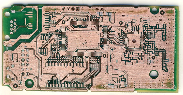
The controller running your production line is failing, its original manufacturer folded years ago, and nobody can find the CAD files. That gap — a working board with no design data — is exactly where PCB reverse engineering earns its place: recovering fabrication-ready files from a physical board so the assembly can be rebuilt, sustained or improved instead of scrapped with the machine.
This guide walks through the workflow, the deliverables you should expect to receive, the legal line that separates legitimate data recovery from cloning, and the verification steps that protect you before committing to volume production. It also covers the honest limits — because not every board should be reverse engineered, and knowing when to redesign instead is part of the service.
Table of Contents
- What PCB Reverse Engineering Actually Involves
- When It Is Legitimate — and When to Walk Away
- The Deliverable Set: What You Should Receive
- The Data Recovery Workflow, Step by Step
- Reaching Inner Layers Without Losing Registration
- Verification: Prove the Data Before You Pay for Volume
- Where PCB Reverse Engineering Hits Its Limits
- Cost and Schedule Logic in Relative Terms
- Choosing a Partner: Questions to Ask and Red Flags
- PCB Reverse Engineering: Key Takeaways
- FAQ
- Have a Legacy Board That Needs New Life?
What PCB Reverse Engineering Actually Involves
PCB reverse engineering is the systematic recovery of a board’s design data from the physical article: the copper layouts of every layer, the drill and via map, the bill of materials, and the connectivity between them. The output is a fabrication-ready file set — Gerber and drill data, a BOM, a netlist and a fabrication drawing — that a manufacturer can build from without ever seeing the original CAD files.
It is worth separating this from what the term sometimes gets confused with. This is not chip-level work: firmware extraction from programmed devices, decapsulation or die analysis are different disciplines with different legal exposure, and they are out of scope here. Likewise, reverse engineering a board is not the same as counterfeiting one — the difference is authorization, which the next section makes concrete.
The contrast with forward design is simple. Forward design starts from requirements and produces a board; reverse engineering starts from a board and recovers the design. The first is creation, the second is restoration — and restoration is what legacy equipment sustainment usually needs.
When It Is Legitimate — and When to Walk Away
The legal test is ownership and authorization, not the technology. Recovering data from a board you own, or from a customer’s board with the design owner’s written authorization, is standard engineering practice for equipment sustainment. Copying a branded product to sell as your own is not, regardless of how the data was obtained. Reputable manufacturers put the authorization step first — before any work starts — and a supplier who never asks should be a warning in itself.
| Situation | Verdict | What to require |
|---|---|---|
| Your own discontinued product, design files lost | Legitimate | Internal records confirming design ownership |
| Customer-owned board, authorized repair or sustainment | Legitimate | Written authorization from the design owner |
| Obsolete industrial spare, machine owner requests rebuild | Legitimate | Proof of equipment ownership and signed authorization |
| Copying a branded consumer product to resell | Not legitimate | Decline — trademark and design-right exposure |
| Relabeled or counterfeit boards entering the supply chain | Not legitimate | Decline — no authorization can cure this |
The practical rule for buyers: be ready to state, in writing, that you own the board or hold the design owner’s authorization to reproduce it. Serious suppliers will ask, keep the declaration on file, and decline work that fails the test — which protects your supply chain as much as it protects theirs.
The Deliverable Set: What You Should Receive
A professional job does not end with a reconstructed picture — it ends with a file set another engineer could quote and build from. The deliverables below are the standard expectation, and each has a verification step attached that you can (and should) run before paying for production.
| Deliverable | What it contains | How to verify it |
|---|---|---|
| Gerber + drill files | Copper layers, soldermask, silkscreen, drill and rout data in standard Gerber format | View in any Gerber viewer; check layer count, board outline and hole sizes against the physical board |
| Bill of materials | Reference designators, package codes and part numbers with alternates for obsolete items | Cross-check against component inventory removed from the board |
| Netlist | Every pad-to-pad connection extracted from the copper geometry | Compare against a flying-probe or bench continuity test of the original board |
| Fabrication drawing | Stackup, layer sequence, thicknesses, finish, impedance callouts where specified | Review against a cross-section of the original board |
| Pick-and-place file | Component centroids and orientations for assembly | Dry-run against board photographs taken before stripping |
Gerber is the exchange format every fabricator accepts — the specification is maintained publicly by Ucamco, and you can read how the Gerber format is defined and versioned if your team wants to validate the files themselves. If a supplier offers to deliver only their proprietary project files and not open Gerber data, push back: you need the open set to stay supplier-independent.
The Data Recovery Workflow, Step by Step
The workflow is sequential, and skipping the early documentation steps is the most common cause of rework. Components carry information — reference silkscreen, orientation, board-history stickers — that disappears the moment heat touches them, so a disciplined job photographs and records everything before the first component comes off.
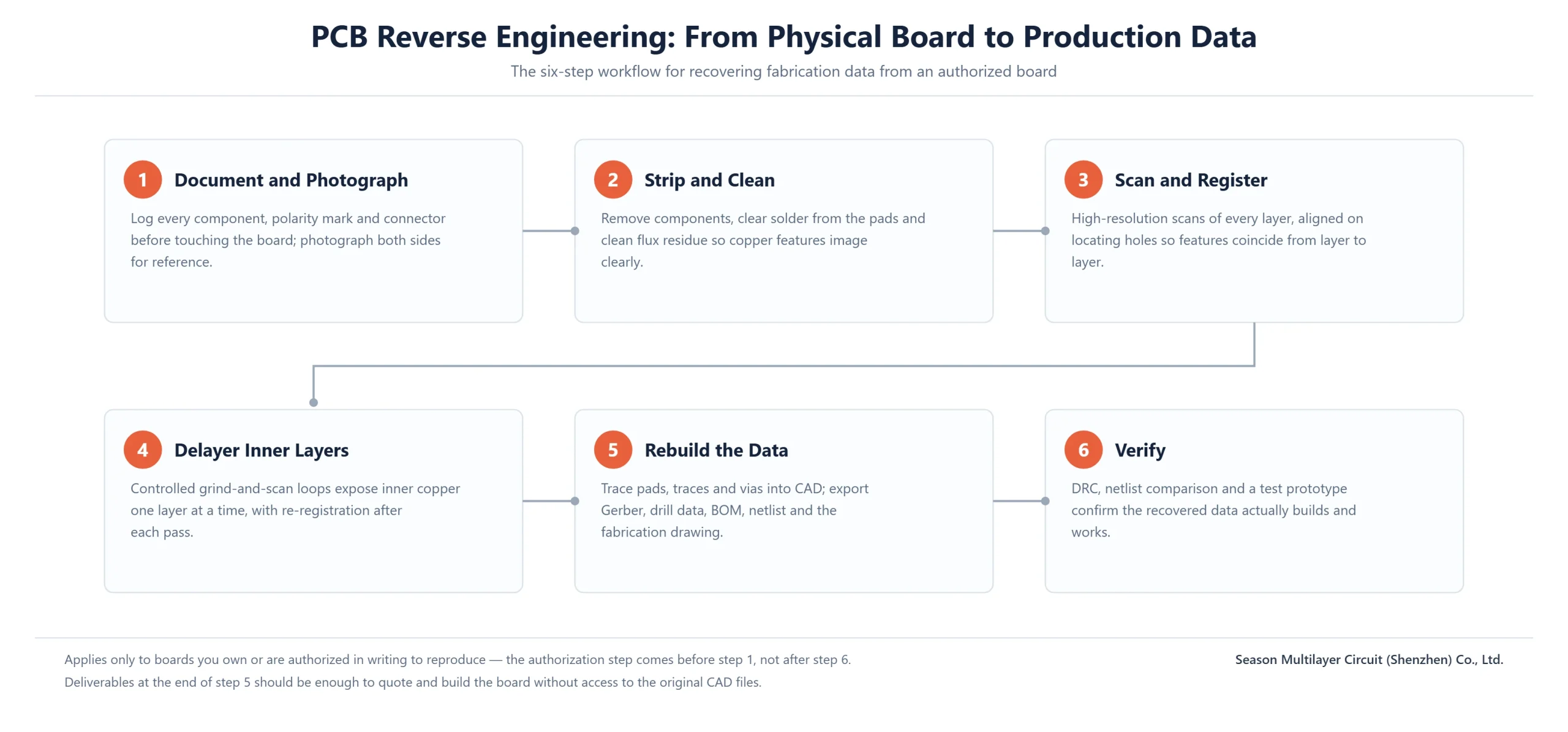
Two properties of the workflow matter to a buyer. First, it is partly destructive: reaching inner layers means removing material, so a sacrificial sample board is preferable if one exists. Second, every layer scanned must be re-registered against the others — layer images aligned on locating features — or the reconstructed data will build a board that looks right and connects wrong.
Reaching Inner Layers Without Losing Registration
Outer layers are straightforward: after cleaning, high-resolution scans (1200 DPI or better is typical) capture the copper pattern, and alignment is checked by verifying that pads and vias coincide between top and bottom images. Inner layers are the hard part, because the copper is buried under laminate and must be exposed layer by layer.
The standard approach is controlled mechanical delayering: the board is ground down in shallow passes, each pass followed by a scan, until the target inner copper is exposed. A four-layer board follows the same loop twice for its two inner layers. Registration discipline decides the outcome — layer images are aligned on locating holes and diagonal reference features, with layer-to-layer position held within roughly 0.1 mm, because drift at this stage becomes shorts or opens in the rebuilt data.
Effort scales sharply with layer count. Doubling the layers does not double the work — it multiplies it, because each intermediate layer must be exposed, scanned and re-registered without damaging the layers still underneath. This is one reason the cost conversation later in this article is about complexity, not just area.
Verification: Prove the Data Before You Pay for Volume
Recovered data is a hypothesis until it is tested. The cheapest tests are electrical: a design-rule check on the reconstructed geometry catches impossible clearances, and a netlist comparison — extracted connectivity versus a continuity test of the original board — catches swapped connections that no visual check will find. Both should be included by default, not offered as extras.
The decisive test is a prototype build. A first article fabricated from the recovered files, assembled and functionally tested against the original board’s behavior, closes the loop. For boards with controlled impedance, the rebuild should include coupon verification, because the recovered stackup can reproduce geometry without reproducing the original dielectric properties exactly. Acceptance criteria should be stated up front — typically IPC-A-600 Class 2 or Class 3 workmanship, per the acceptance standards in the IPC standards library.
Insist on receiving the verification evidence, not just a pass/fail statement: the netlist comparison result, the cross-section photographs and the test report belong in your file alongside the deliverables. They are your baseline for every future rebuild.
Where PCB Reverse Engineering Hits Its Limits
Some recoveries are partial by nature, and a trustworthy supplier says so at the review stage rather than after your deposit. The limits cluster in three areas: micro-geometry, materials and programmed content.
Micro-geometry is the first. Advanced HDI builds — stacked and staggered laser microvias down to 0.1 mm, fine-line outer layers, buried via structures — can be imaged, but reproducing the exact drill registration and plating fill from optical analysis alone is unreliable. For these builds the practical recommendation is usually a redesign with equivalent function rather than a clone: our HDI PCB technology guide explains what the fabricator actually controls, and why advanced HDI manufacturing challenges make cloning particularly risky.
Materials are the second. A recovered stackup reproduces layer geometry and copper weights, but the original laminate brand, resin content and glass style must be inferred — which is why impedance on the rebuilt board is verified by coupon rather than assumed. Programmed devices are the third: a reverse-engineered board recovers its connectivity, not its firmware, so a working firmware image or a re-programming path must come from your side.
Cost and Schedule Logic in Relative Terms
Reverse engineering carries a one-time engineering charge that has nothing to do with the per-board price of the rebuilt article. That charge scales with complexity — layer count, pad density, component count and the number of package types — not with board area. For a simple double-sided board it is modest; for a dense multilayer it can exceed the cost of the first prototype build itself, sometimes by several times.
The economics work when the recovery is amortized: the engineering cost is paid once, then every subsequent rebuild batch runs at normal production pricing. Sustainment programs that need the board for years almost always clear that bar; a one-off replacement usually does not, and in that case buying engineering time to redesign a simplified equivalent may serve you better. Our 4-layer PCB cost breakdown shows how the rebuilt board’s production quote is structured once the data exists.
On schedule, treat the timeline as an engineering review outcome rather than a fixed number: feasibility confirmation, the delayering loop, data rebuild and a prototype build each carry their own variables. A supplier who quotes a recovery timeline before seeing the board is guessing; ask for the review first.
Choosing a Partner: Questions to Ask and Red Flags
The supplier landscape ranges from fabrication houses with in-house engineering teams to intermediaries who subcontract everything. Five questions separate them quickly:
- What do you require as authorization, and at what point in the process do you require it?
- Which deliverables are standard — and will I receive open Gerber data, not just project files?
- Is netlist comparison and DRC included, or quoted separately?
- Can you build, assemble and test the prototype from the recovered data under the same roof?
- Who owns the recovered data files once the job is paid for?
Red flags mirror the questions: no authorization request, no verification step in the quote, proprietary-only file delivery, or reluctance to hand over source data you paid for. Integration is the quiet differentiator — a supplier who fabricates and assembles, like the teams behind our industrial control PCB and security system PCB builds, closes the loop from recovered data to a tested board without a second handoff.
PCB Reverse Engineering: Key Takeaways
If you are evaluating a recovery project, these are the points that should shape the decision:
- Authorization in writing comes first — legitimate sustainment work passes this test easily, so a supplier who never asks is the risk.
- Judge the deliverable set, not the pitch: Gerber, drill, BOM, netlist and fab drawing, each with a stated verification method.
- The workflow is partly destructive; provide a sacrificial board if you can.
- Verification is the product: netlist comparison, DRC and a tested first article before any volume commitment.
- Know the limits — advanced HDI micro-geometry, exact laminate data and firmware are out of reach, and redesign is often the better answer.
Approached this way, data recovery is not a gray area — it is standard sustainment engineering with clear boundaries, and the suppliers worth using are the ones who make those boundaries explicit.
Frequently Asked Questions
Is PCB reverse engineering legal?
It depends on ownership and authorization, not on the technique. Recovering data from a board you own, or from a customer board with the design owner’s written authorization, is standard sustainment engineering. Copying branded products for resale is not, and reputable manufacturers require a signed authorization statement before starting any work.
What deliverables does PCB reverse engineering produce?
A fabrication-ready set: Gerber and drill files, a bill of materials with alternates for obsolete parts, an extracted netlist, a fabrication drawing with stackup, and a pick-and-place file for assembly. Verification evidence — netlist comparison results, cross-section photographs and test reports — should accompany them.
How accurate is a reverse-engineered multilayer board?
For conventional builds, accurate enough to rebuild and certify: layer images are registered to roughly 0.1 mm, and electrical verification catches connection errors. Accuracy is proven, not assumed — the netlist comparison and a tested first article are what turn recovered data into production data.
Can HDI boards with microvias be reverse engineered?
Partially. Stacked laser microvias down to 0.1 mm and fine-line structures can be imaged, but reproducing exact drill registration and plating fill from optical analysis alone is unreliable. For advanced HDI, a functional redesign with an equivalent stackup is usually the more dependable path than a clone.
How much does it cost relative to a fresh board design?
The recovery carries a one-time engineering charge that scales with layer count and density, and for dense multilayer boards it can exceed the cost of a first prototype build — sometimes several times over. It pays off when amortized across rebuild volume over the years the board stays in service; a one-off replacement rarely justifies it.
What do I need to provide to start a project?
Ideally the physical board plus a sacrificial sample if inner layers are involved, any surviving documentation, and the board’s operating context. If the board cannot leave your site, high-resolution photographs of both sides start the feasibility conversation. A signed ownership or authorization statement is required before work begins.
How is the recovered data verified before mass production?
Through three checkpoints: a design-rule check on the reconstructed geometry, a netlist comparison between extracted connectivity and a continuity test of the original board, and a first-article build that is assembled and functionally tested against the original. Controlled-impedance boards additionally get coupon verification of the rebuilt stackup.
Have a Legacy Board That Needs New Life?
Send photographs of both sides of the board plus its operating context, and an engineering review will confirm feasibility, deliverables and a realistic path to a tested rebuild before any commitment. The manufacturing capability overview shows what the same engineering team handles once the data is rebuilt.