Book Appointment Now

Solder mask selection decided by ink family, thickness over copper, dam width and CTI rather than datasheet headline numbers, with a drawing checklist.
PCB Solder Mask Selection: Ink, Thickness and CTI Checks
Most solder mask selection decisions are made before the panel reaches the imaging line, in a conversation that lasts about ninety seconds and covers only the ink brand and the surface finish. Solder mask selection deserves more than that, because the same ink that performs perfectly on a 1.6 mm four-layer control board will blister on a 0.8 mm HDI build with 0.5 mm pitch lands, and the drawing will not have said anything different in either case.
This guide treats the mask as three separate specifications that have to agree: the ink family, the thickness and geometry it has to hold, and the electrical job it does when creepage distances get tight. Each section gives the number that matters and the way it is checked on the floor. If you are still deciding the dielectric system underneath, the laminate and material guide covers that layer of the decision.
Table of Contents
- What the Solder Mask Actually Has to Do
- Solder Mask Selection Starts With the Ink Family
- Thickness Targets Over Copper, Edges and Pads
- Resolution, Registration and Dam Width
- Adhesion, Cure Window and the Two Failure Modes
- Surface Finish Compatibility
- CTI, Creepage and the Electrical Job
- Tenting, Plugging and What Happens at the Via
- Incoming Checks Before the Ink Reaches the Line
- Solder Mask Selection Checklist for the Drawing
- FAQ
- Put the Mask Requirement on the Drawing, Not in an Email
What the Solder Mask Actually Has to Do
The mask is a permanent polymer coating that stays on the board for its entire life, so it is judged on four jobs at once. It has to insulate between conductors that are closer than the laminate alone would allow, act as a dam that keeps molten solder where the pad is, protect copper from oxidation and handling damage, and survive assembly without cracking, blistering or losing adhesion.
Those jobs pull in different directions. A thicker coat insulates and survives handling better, but it is harder to develop cleanly at fine geometry and more likely to trap solvent. A thinner coat images better at 4 mil dams, but coverage over a 2 oz copper step becomes marginal. Everything in the rest of this article is a consequence of that trade-off.
One clarification that saves arguments later: the mask is not a substitute for the fabrication drawing. If the drawing does not state the ink type, the thickness target, the via treatment and the acceptance criteria, the fabricator will apply its house standard, which is optimised for yield rather than for your assembly process.
Solder Mask Selection Starts With the Ink Family
Four families cover almost everything built today, and the choice is driven by geometry and volume rather than by preference. Photoimageable liquid ink applied by screen printing is the workhorse for multilayer and HDI work. The same chemistry applied by spray or curtain coating suits thin panels and high-mix shops. Dry film mask is laminated as a sheet and imaged, which gives the most uniform thickness. Thermal-cure screen ink is the low-cost option for simple boards, patterned by the screen itself rather than by exposure.
| Ink family | How it is applied | Geometry it holds | Best fit | Where it hurts |
|---|---|---|---|---|
| Photoimageable liquid, screen printed | Screen coat, pre-cure, expose, develop | 4–5 mil dam on 1 oz copper | Multilayer and HDI volume work | Mesh marks and thickness variation across a large panel |
| Photoimageable liquid, spray or curtain coated | Spray or curtain coat, expose, develop | Finer dams on thinner films | Thin panels, dense fine-pitch boards, high mix | Coverage over tall copper steps; needs flat, clean panels |
| Photoimageable dry film | Vacuum lamination, expose, develop | Uniform thickness, fine openings | Fine-pitch HDI where film uniformity matters | Conformability around thick copper and heavy via fill |
| Thermal-cure screen ink | Screen print, oven cure, openings set by the screen | Coarse openings, wide dams | Simple double-sided and low-density boards | Registration on fine pitch, limited tenting of small vias |
Two practical rules follow from the table. First, never compare inks by datasheet numbers alone, because the datasheet describes a 25 micron film on smooth copper, not the 15 micron film you will get over a trace edge. Second, if the board mixes heavy copper with fine pitch, no single coat does both well and the conversation should move to which region can accept a compromise.
Thickness Targets Over Copper, Edges and Pads
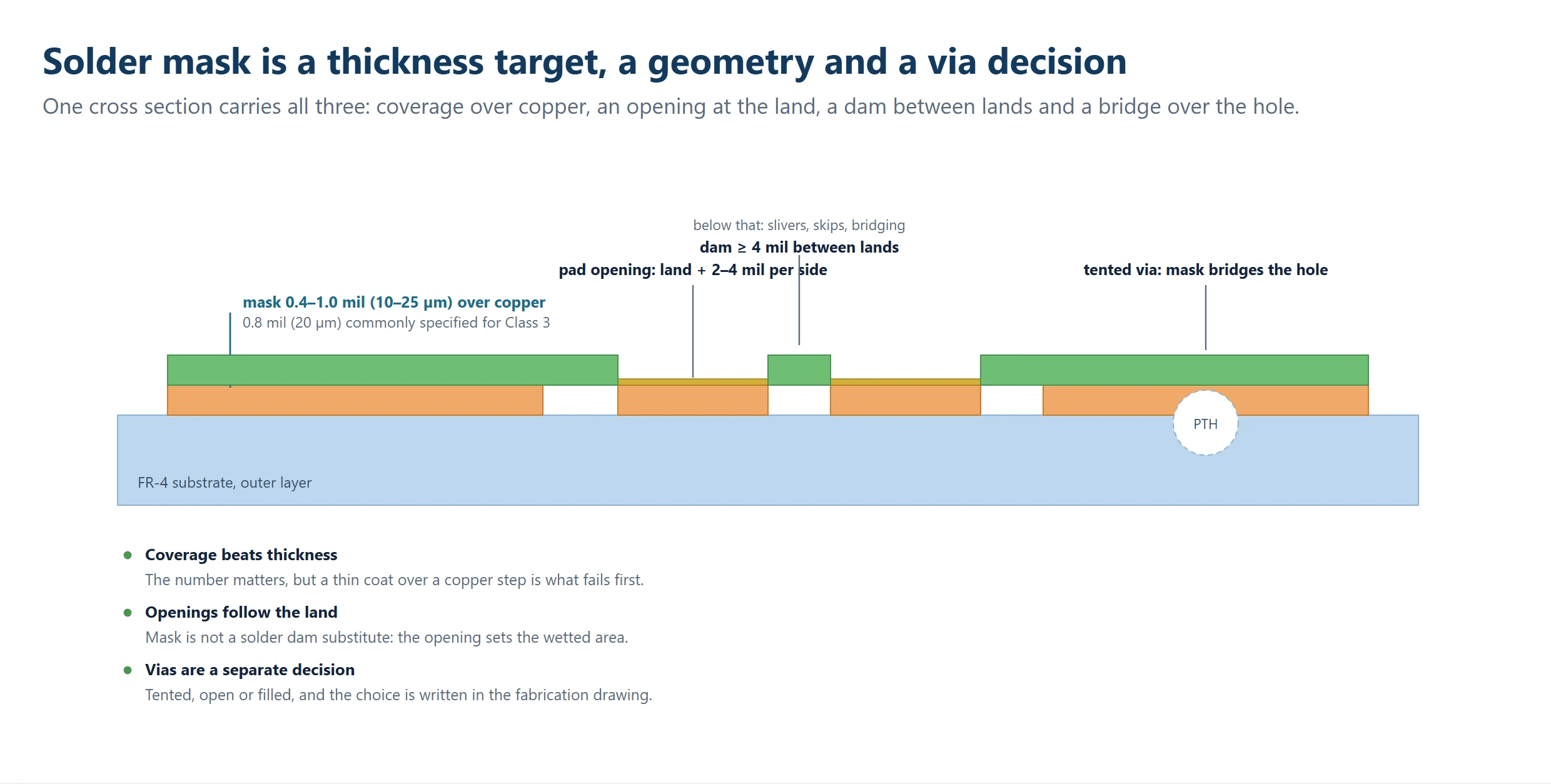
Thickness is specified on the finished board over the conductor, not on the wet film. A common floor is 0.4 mil (10 µm) over conductor edges, with Class 3 work frequently calling for 0.8 mil (20 µm) and above. Confirm the figure in your own acceptance standard rather than assuming the house number, since the standard you cite in the purchase order is what an inspector will measure against.
| Location on the board | Typical target | Why it is specified there | How it is verified |
|---|---|---|---|
| Over a conductor on the outer layer | 0.4 mil (10 µm) minimum; 0.8 mil (20 µm) for Class 3 work | Insulation and resistance to handling damage | Microsection on a coupon, or an optical thickness gauge |
| At a land opening | No ink on the land; opening 2–4 mil larger than the land per side | Sets the wetted area and the solder fillet shape | First-article visual against the drawing, then AOI |
| Between two lands (dam) | 4 mil (0.1 mm) minimum, and pitch-limited | Prevents solder bridging between adjacent pads | AOI with dam width measurement at the tightest pitch |
| Over a tented via | Full coverage with 0.5 mil over the rim | Stops flux and contamination entering the barrel | Visual and cross-section on the qualification coupon |
| At the board edge and rout | 5–10 mil clearance from the rout path | Stops the mask flaking along a machined edge | Visual at the array frame |
The number people forget is the one over a copper step. On a heavy copper board the mask film thins dramatically as it drapes over the trace shoulder, so a nominal 25 micron coat can measure 8 microns at the edge. If the drawing asks for coverage over 2 oz copper, say so explicitly and let the fabricator choose a coat weight that survives the step.
Resolution, Registration and Dam Width
Dam width is the single most useful capability question, because it combines ink resolution, imaging exposure and registration in one number. Ask what the minimum dam is at your copper weight and pitch, not what the ink datasheet claims. A shop that holds 4 mil dams reliably on 0.5 mm pitch is telling you something concrete about its exposure and development control.
Registration is the other half. The mask opening has to sit concentrically on the land, and on a 0.4 mm pitch array there is very little room for error before the opening covers part of the neighbouring land and creates a bridge risk. Registration is limited by the lamination and imaging alignment, not by the ink, which is why the same ink behaves differently on panels of different size.
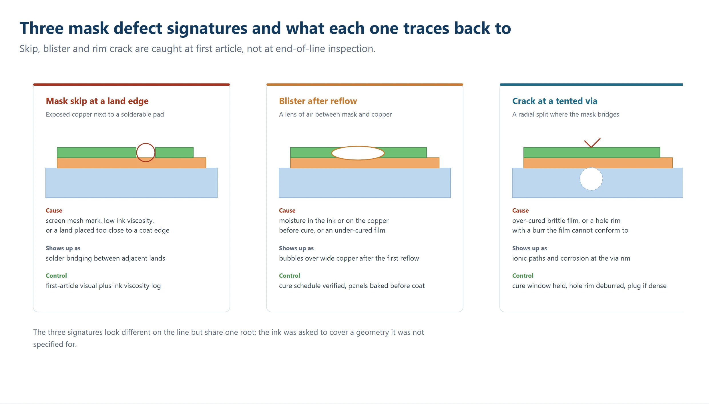
Below about 4 mil, dams start to fail in a characteristic way: a sliver of ink lifts during development, the opening merges with its neighbour, and the board passes visual inspection in one orientation while bridging at reflow. If a design needs dams under that width, the correct answer is usually a different pad geometry or a change of pitch, not a thinner ink.
Adhesion, Cure Window and the Two Failure Modes
Almost every field failure I have seen on mask traces back to cure, in one direction or the other. Under-cure leaves residual solvent and unreacted photoinitiator, which shows up as ionic contamination, patchy adhesion and occasionally as a dull, uneven surface after reflow. Over-cure makes the film brittle, so it cracks at via rims and along rout edges when the panel is depanelised.
The objective evidence is boring and effective: a cure schedule held inside a documented window, a tape peel or cross-hatch on the first article, pencil hardness on a coupon, and an ionic contamination measurement on the finished panel. Ask for the cure window in the process control plan and then ask what the operator does when a panel is double-passed through the oven, because that is where the window usually gets lost.
Adhesion also depends on what is underneath. Oxide treatment, micro-etch depth and surface cleanliness before coating determine whether the film keys to copper or merely sits on it. A board that passes every measurement on a smooth test coupon can still fail adhesion over a brushed, contaminated production panel.
Surface Finish Compatibility
The mask sees the finish chemistry and the assembly thermal profile, so the pair has to be specified together. This is where a technically adequate ink becomes an inadequate choice.
| Surface finish | What it does to the mask | What to specify |
|---|---|---|
| Lead-free HASL | Molten solder near 260–270 °C plus a hot-air wipe; the harshest thermal event in common use | Ink rated for the thermal excursion, and a thickness that survives the wipe without thinning at the land edge |
| ENIG | Alkaline and acid baths at 80–90 °C over several transfers | Chemical resistance, plus adhesion checked after the full plating cycle rather than before it |
| Immersion silver or immersion tin | Mildly acidic, short dwell, low thermal load | Standard photoimageable liquid ink; watch for staining at mask edges |
| OSP | Acidic, low temperature, no thermal shock | Confirm the ink is compatible with the acid cleaner, then treat it as a low-risk pairing |
| Hard gold on edge fingers | Plating, taping and tape removal over a masked surface | Ink that resists tape peel; fingers are usually masked off and plated separately |
ENIG deserves a note because the failure is so often blamed on the wrong layer. A board can show poor solder wetting that looks like a mask issue when the real cause is the nickel bath, which is covered in this ENIG solderability and black pad analysis. Check which layer failed before changing the ink.
CTI, Creepage and the Electrical Job
On mains-connected and industrial boards the mask stops being cosmetic and becomes part of the insulation coordination. Comparative tracking index describes how a material resists forming a conductive carbon path across a wet, polluted surface, and the mask film sits directly in that path between two conductors.
The important subtlety is that the ink does not upgrade the laminate. If the base material is rated for one tracking class and the ink for a better one, the assembly is limited by the weaker of the two along any path that crosses bare laminate, for example in a mask opening or at a board edge. Where creepage distances are tight, specify a tracking-improved ink and confirm the laminate class at the same time, following the spacing logic in this CTI ratings and creepage guide.
For products above roughly 300 V working voltage, write the requirement into the drawing as a material property with the standard cited, for example the spacing rules of IEC 60664-1, and ask the fabricator for the ink’s tracking data. A generic claim of good insulation is not something an inspector can check.
Tenting, Plugging and What Happens at the Via
Via treatment is a separate decision from mask type and is the most commonly unstated item on a fabrication drawing. Tenting covers the hole with mask during the normal coat. Plugging fills the barrel with resin or ink before or after coating. Leaving the via open is the third option, and it is legitimate when the via is used as a test point or when outgassing during assembly must be avoided.
Tenting works well down to about 0.3 mm and starts to fail below that, because the film cannot bridge the hole without support and sags into the barrel during cure. Dense via fields on a thin board are the worst case: the film stretches over many holes at once and cracks at the rims. The comparison between the two treatments is set out in this tenting versus plugging comparison, and the resin-versus-ink choice for plugged vias is covered in the via plugging materials guide.
For via-in-pad the decision is already made for you: the via must be filled and planarised, because a tented via under a component pad will cause voiding or an open joint. That process belongs with the plating and fill step, not with the mask.
Incoming Checks Before the Ink Reaches the Line
The mask is a purchased chemical, and it deserves the same incoming discipline as laminate. Four checks catch nearly all of the problems that would otherwise appear as random line defects.
- Lot certificate matching the ink part number, batch and date, with a shelf life that has not expired.
- Viscosity measured against the process window on receipt, not only when a defect appears.
- Storage and mixing conditions recorded, including the pot life clock once the hardener is added.
- First-article verification on a production coupon: cross-hatch adhesion, thickness, dam width and cure hardness.
Then close the loop with the acceptance criteria in the same document. The workmanship requirements for mask integrity, coverage and marking should reference a published standard such as the IPC criteria at Global Electronics Association, while the flammability and material ratings come from the supplier’s UL record. Two references, two different questions.
Solder Mask Selection Checklist for the Drawing
The drawing is the only place where all of this survives. Put the six items below on it and most of the arguments disappear before the first panel is coated.
| Drawing item | What to write | Why it matters |
|---|---|---|
| Ink family | Photoimageable liquid, applied by screen or spray | Sets resolution, thickness range and cost level |
| Thickness | 0.4 mil minimum over conductor edges; 0.8 mil for Class 3 areas | Gives the inspector a measurable target |
| Dam width | State the minimum acceptable dam at the tightest pitch | Converts geometry into a pass or fail decision |
| Via treatment | Tented, open or filled and planarised, by via size | Removes the most common silent default |
| Tracking requirement | Tracking index or class, plus the reference standard | Makes an electrical property verifiable |
| Acceptance standard | Class 2 or Class 3 per the workmanship standard you cite | Aligns the visual criteria with the rest of the drawing |
If only one item can be added, make it the via treatment. It is the field that most often changes without anyone noticing, and the one whose absence produces the most expensive late discovery.
Frequently Asked Questions
What is the minimum solder mask thickness over a trace?
0.4 mil, or 10 microns, over the conductor edges is the common floor, and Class 3 work is often specified at 0.8 mil or 20 microns. Measure on the finished board rather than the wet film. Over a heavy copper step the film thins sharply at the trace shoulder, so a nominal coat can fall below the minimum right where it matters.
How wide does a solder mask dam need to be?
Four mil, roughly 0.1 mm, is the practical minimum for a stable dam, and it depends on both copper weight and pitch. Below that, slivers lift during development and adjacent openings can merge, which shows up as solder bridging at reflow rather than at inspection. If the design needs less, change the pad geometry instead of the ink.
Is LPI the same as photoimageable solder mask?
LPI stands for liquid photoimageable, so yes in everyday usage, but the application method still matters. The same chemistry screen printed and spray coated behaves differently over copper steps and on thin panels. When a supplier says LPI, ask how it is applied before accepting the capability claim.
Does the solder mask affect CTI values on the board?
It can, on any path where the tracking route crosses the mask film, but it cannot improve the laminate underneath. If the base material is in a lower tracking class, a better ink does not raise the assembly’s rating along paths crossing exposed laminate. Specify both properties and confirm which one governs each gap.
Why does the mask blister after reflow but look fine before?
Moisture is the usual cause: solvent left in an under-cured film, or water absorbed on the copper before coating, expands at reflow temperature and lifts the film. Over wide copper areas the effect is strongest because there is more trapped volume. Bake panels before coating and hold the documented cure window.
Can a tented via be used under a component pad?
No. A tented via under a land will trap air and flux during assembly, which produces voids or an open joint. Vias inside pads must be filled and planarised before the mask step, and the fill belongs to the plating process rather than to the coating line.
Which mask defects should a buyer check at first article?
Four: a dam width measurement at the tightest pitch, cross-hatch adhesion on a production coupon, thickness over a conductor edge, and a cross-section through a tented via. Those four cover the geometry, the chemistry and the via treatment, which is where nearly all field failures originate.
Put the Mask Requirement on the Drawing, Not in an Email
Send the stackup with the tightest pitch, the copper weight and the assembly thermal profile, and the engineering team will come back with the ink family, the thickness target and the via treatment that fit your build rather than the shop default.
The manufacturing services overview shows how coating, imaging and finish steps are sequenced, which is useful when a mask change has to be coordinated with the finish specification.