Book Appointment Now

What a 6-layer industrial control PCB involves: a real production spec sheet, stackup and laminate reasoning, IPC class, test flow, lead times and cost drivers.
6-Layer Industrial Control PCB: Specs, Stackup and Sourcing
Industrial buyers rarely get excited about a board until it fails in the field: a drive that reboots in summer heat, a controller that drifts after two years of continuous duty, a retrofit that needs a replacement board a decade after the original run. The 6-layer industrial control PCB sits right in that risk zone — complex enough to need shielded inner routing and a proper power distribution pair, durable enough to run around the clock in dusty enclosures, and expected to stay orderable far longer than a consumer product cycle. This article walks through one real production case from our floor: the full specification sheet, why each parameter was chosen, how the stackup supports reliability, which tests run before shipment, and what actually drives cost and lead time. Use it as a benchmark when you compare quotes — if a supplier cannot state these numbers for a comparable build, that silence is the first finding.
Table of Contents
- What Is a 6-Layer Industrial Control PCB?
- Specifications From a Real Production Build
- Stackup and Laminate Choice for Industrial Environments
- What Separates Industrial Reliability From Consumer Grade
- Where 6-Layer Industrial Control PCBs Are Used
- Quality Control From Prototype to Volume
- Lifecycle, Reorders and Engineering Data Retention
- What Drives the Cost of a 6-Layer Industrial Control PCB
- Prototype and Volume Lead Times, and What to Confirm
- FAQ
- Benchmark Your Board Against This Spec Sheet
What Is a 6-Layer Industrial Control PCB?
A 6-layer industrial control PCB is a six-copper-layer laminate built for controllers, drives, instrumentation and similar equipment that runs for years in factory conditions. Compared with a four-layer consumer board, the two extra layers buy a shielded inner signal layer between planes, a dedicated power distribution pair, and enough routing density to fan out a mid-size processor without condensing the board. The term “laser” that often appears alongside this board class refers to the application — control boards for laser-based industrial equipment — not to laser-drilled microvias; the case documented here is a conventional through-hole build with mechanical drilling only.
What actually defines the class is the reliability envelope: wide operating temperature, continuous duty, resistance to dust and vibration, and a supply commitment measured in years rather than seasons. Those requirements shape the laminate choice, the copper weights, the acceptance class and the test flow — and they are the reason an industrial quote looks different from a consumer one even when the layer count matches.
Specifications From a Real Production Build
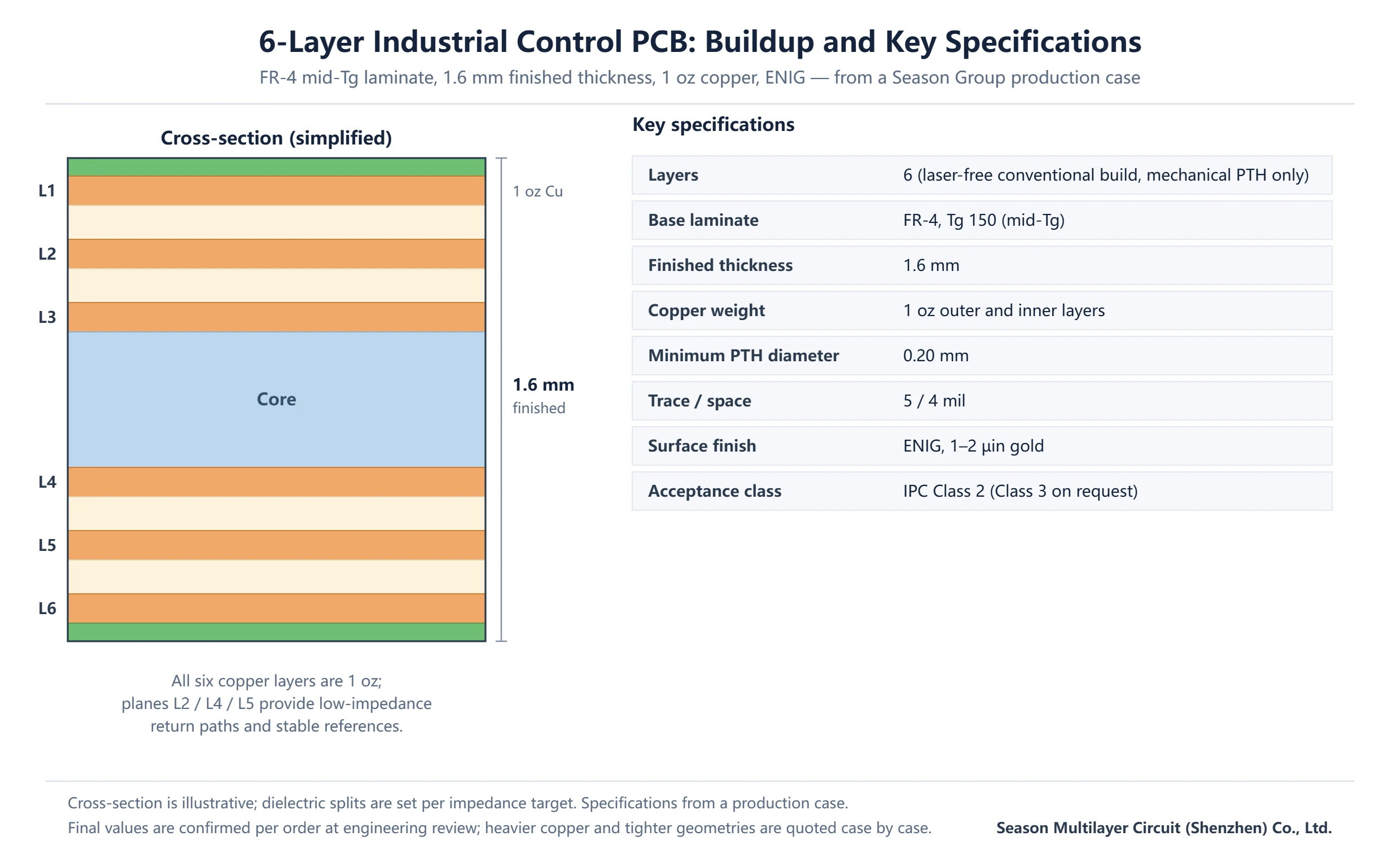
The table below is the specification sheet of a produced case, manufactured to the customer’s Gerber data for a laser-equipment control application. Every value here is one a supplier should be willing to state — and defend — for a comparable design.
| Parameter | Specification | Why it was chosen |
|---|---|---|
| Layer count | 6 layers | Inner shielded routing plus a dedicated power pair without the cost of an 8-layer build |
| Base laminate | FR-4, Tg 150 (mid-Tg resin system) | Handles continuous elevated operating temperature at standard FR-4 processing cost |
| Finished thickness | 1.6 mm | Standard card-edge and connector interfaces; adequate stiffness for enclosure mounting |
| Copper weight | 1 oz outer and inner layers | Carries supply rails and motor-drive currents without resorting to heavy-copper processing |
| Minimum PTH diameter | 0.20 mm | Mature mechanical drilling; reliable plating at standard aspect ratio |
| Trace / space | 5 / 4 mil | Comfortable geometry for controller fanout with high etch yield |
| Surface finish | ENIG, 1–2 µin gold | Flat, solderable, corrosion-resistant pads for fine-pitch devices and long storage |
| Acceptance class | IPC Class 2 (Class 3 on request) | Matches industrial expectations; Class 3 reserved for safety-critical hardware |
Note what is absent from this sheet: no exotic material, no microvia structure, no unusual plating. A well-designed industrial board concentrates the budget where reliability lives — laminate grade, copper weight, plating quality and inspection depth — rather than in headline geometries.
Stackup and Laminate Choice for Industrial Environments
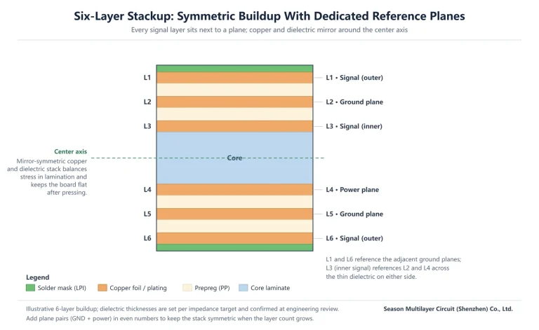
The stackup follows the standard six-layer arrangement: outer signal layers, an inner signal layer, and three plane layers (two ground, one power) arranged symmetrically around the center core. Symmetry is not cosmetic — mirror-symmetric copper and dielectric distribution keeps lamination stress balanced so the panel stays flat through pressing and double-sided reflow. Our balanced stackup and warpage control guide covers the mechanics, and the PCB materials and laminates guide explains how resin systems differ across grades.
The Tg 150 designation deserves precision. It is a mid-Tg FR-4: glass transition at 150 °C, well suited to continuous industrial operating ranges, processed with standard parameters. It is not a specialty high-temperature system, and specifying one without a thermal justification only narrows the supplier pool and lengthens lead time. For this build the resin system also needed proven compatibility with ENIG plating and with the customer’s reflow profile — both confirmed at engineering review before panel cutting. Material trade-offs across FR-4 grades are compared in our FR-4 laminate selection guide.
What Separates Industrial Reliability From Consumer Grade
On paper a consumer board and an industrial board can share a layer count and even a thickness. The difference is in the envelope each is designed against — temperature span, duty cycle, service life and the acceptance criteria enforced during inspection.
| Dimension | Industrial control PCB | Consumer-grade PCB |
|---|---|---|
| Operating temperature | Approximately −20 °C to +85 °C | Approximately 0 °C to +60 °C |
| Duty cycle | Continuous, 7×24 operation | Intermittent use |
| Acceptance class | IPC Class 2, Class 3 on request | Class 1 or Class 2 |
| Supply commitment | Spare boards orderable for 5–10 years | Product cycle of 1–2 years |
| Relative cost | ≈ 1.2–1.5× the consumer equivalent | Baseline |
The cost ratio in the last row is the honest framing: industrial builds carry roughly a 20–50% premium over a consumer equivalent of the same size, paid for in laminate grade, test depth and process control. Buyers who compress that premium by relaxing the acceptance class usually pay it back in field failures, where the arithmetic is far worse.
Where 6-Layer Industrial Control PCBs Are Used
The board class spans a wider range than the name suggests. The table lists the sectors we see most often, with the stackup demand that dominates each one.
| Sector | Typical boards | Dominant stackup demand |
|---|---|---|
| Laser equipment | Laser source controllers, motion and safety interlock boards | Isolation between power drive sections and control logic; wide-temperature laminate |
| Factory automation | PLC main boards, motion control, data acquisition cards | Dense processor fanout on inner layers; continuous-duty copper weights |
| Power and energy | Inverter control boards, distribution monitoring | Creepage and clearance in power regions; reinforced supply routing |
| Instruments | Measurement and analysis main boards | Low-noise references for analog sections; shielded inner signal routing |
| Robotics and machinery | Robot controller boards, drive electronics | Vibration-tolerant mounting; thermal headroom for enclosed cabinets |
Across all five sectors the pattern repeats: the six-layer build is chosen when a four-layer board cannot hold both the routing density and the plane structure the application needs, but the geometry still fits standard processing. Once fine-pitch BGA fanout or high-speed serial links push further, designs graduate to HDI constructions — a produced 10-layer HDI industrial control PCB shows that next step in the same product family.
Quality Control From Prototype to Volume
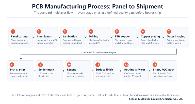
The inspection flow for this class runs on two tracks: every board and every batch. On the board track, automated optical inspection screens each layer for etch defects, followed by 100% electrical test — flying probe on prototypes and low-volume runs, fixture or ICT testing where volumes justify the tooling. First-article cross-sections confirm plated hole copper and surface copper thickness against the specification, and test reports ship with the goods.
On the batch track, key process steps are monitored statistically so drift is caught between lots rather than inside them. Where the application justifies it — medical-adjacent instrumentation, safety-relevant drives — customers can add reliability verifications such as temperature cycling, insulation-resistance and hipot testing, with impedance verified by TDR on the production coupon. Each verification is data-logged per batch, which is what later sustains audits and repeat-order comparability.
Lifecycle, Reorders and Engineering Data Retention
Industrial equipment outlives its development cycle by a wide margin, so the supply question is not whether a reorder will come but when — and whether the board built five years later still matches the original. That is an engineering-data discipline: layer stackup, material designators, impedance coupons, drill files and process parameters are archived per project, so a reorder re-releases from the stored program instead of being re-engineered from scratch.
For buyers this has a practical consequence: keep your fabricator’s archive reference in your own records, and prefer suppliers who state their retention practice in writing. When the day-one build and the year-eight spare are traceable to the same data set, second-source qualification and field-repair decisions both get dramatically simpler. Group-level capacity matters here too — our three plants and 3,000,000 m² of annual capacity exist precisely so that a product family is not hostage to one production line.
What Drives the Cost of a 6-Layer Industrial Control PCB
Board cost at this layer count is dominated by five levers, in roughly descending order: panel utilization (how many boards fit a production panel with acceptable breakaway), laminate grade, surface finish, copper weight, and the tightness of the minimum trace/space and hole geometry. None of these is hidden — a quote should itemize them, and a buyer comparing quotes should normalize them first, because two offers with the same headline number can differ by a class in one of these levers.
| Cost lever | What moves it | Typical relative effect |
|---|---|---|
| Layer count | 4 → 6 layers adds two copper foils, a lamination step and more drilling | ≈ +30–60% vs a 4-layer equivalent |
| Laminate grade | Mid-Tg FR-4 baseline; specialty systems raise material and processing cost | Baseline choice; upgrades quoted case by case |
| Surface finish | ENIG carries a premium over HASL; justified by fine pitch and shelf life | Moderate premium, stable across volumes |
| Copper weight | Heavy copper needs plating time and affects etch yield | Noticeable above 2 oz |
| Acceptance class | Class 3 adds inspection depth and documentation | Quoted per requirement |
The practical way to hold cost is to spend where the application is exposed — laminate grade and copper weight for an industrial build — and to keep geometry inside comfortable processing windows where it is not. A high-reliability 8-layer security system PCB in our portfolio shows the same philosophy one tier up.
Prototype and Volume Lead Times, and What to Confirm
For a conventional six-layer build like the case above, prototype runs typically complete in 5–7 working days and volume production in 15–20 working days, confirmed at engineering review for the specific stackup, copper weight and test scope. Two factors move those numbers most: engineering-review duration (how quickly stackup and DFM questions get answered) and test depth, since 100% electrical testing and any added reliability verification schedule into the calendar.
The fastest path through review is complete data: Gerber data including the drill layer, the stackup table, impedance targets and the acceptance class. That single package lets engineering answer manufacturability, test scope and delivery in one pass. Rushed scheduling is possible on conventional builds, but the honest sequence is to let the engineering review set the date — a committed schedule with the process scope stated is worth more than an optimistic promise made before the data is read. Data exchange formats such as Gerber are maintained openly, so there is no reason for ambiguity on the design side; the IPC standards family covers the acceptance criteria on the fabrication side.
Frequently Asked Questions
What files do I need to get a 6-layer industrial control PCB quoted?
Gerber data including the drill layer, plus a stackup table with layer functions, material designators, copper weights and impedance targets, and the required acceptance class. With that package an engineering team can return DFM comments, a test plan and a production schedule in one review pass instead of trading questions over several days.
Why is Tg 150 FR-4 common on industrial control boards?
A Tg 150 mid-Tg FR-4 covers continuous elevated operating temperatures and standard reflow profiles while keeping material cost and processing in the standard FR-4 window. It is a reliability-per-cost choice: specialty high-temperature laminates are justified only when the thermal analysis actually demands them, and they narrow the supplier pool when they are not needed.
How long do prototype and production runs take?
A conventional six-layer industrial build typically completes prototypes in 5–7 working days and volume production in 15–20 working days, with the exact schedule confirmed at engineering review. Review speed and test depth are the two biggest variables, so complete data (drill files, stackup, impedance targets, acceptance class) is the fastest way to protect the calendar.
What tests are performed on industrial control PCBs?
Standard scope: automated optical inspection on every layer, 100% electrical test by flying probe or fixture, first-article cross-sections for hole copper and surface copper, and impedance verification by TDR on production coupons. Temperature cycling, insulation-resistance and hipot testing can be added per customer specification for critical applications, with results data-logged per batch.
Can these boards be built to IPC Class 3?
Yes. The case in this article ships as IPC Class 2, which matches most industrial equipment, and Class 3 acceptance is available on request for safety-critical hardware. Class 3 tightens plating thickness, inspection criteria and documentation, so state the requirement at quoting — it affects both process scope and cost, and retrofitting it later is not practical.
How is quality kept consistent from prototypes to volume?
Prototype and volume runs release from the same archived engineering program: identical stackup data, drill files and process parameters. First-article confirmation gates the transition, key process steps are monitored statistically between lots, and cross-section plus test data is archived per batch so any later reorder reproduces the original build rather than re-engineering it.
Is submitted design data kept confidential?
Submitted files are used only for production review and manufacturing, access is restricted to the engineering team handling the project, and non-disclosure agreements can be signed on request. Production data is archived to support reorders and can be scheduled for destruction per agreement — the archive reference belongs to the customer’s project, not to a data pool.
Benchmark Your Board Against This Spec Sheet
Season Multilayer Circuit (Shenzhen) Co., Ltd., part of the 998 PCB Group founded in 2006, builds industrial control boards from 2 to 30 layers across three plants with 3,000,000 m² of annual group capacity. Submit your Gerber data and stackup requirements through our PCB manufacturing services page and compare our engineering review — specification confirmation, DFM comments and a committed schedule — against any quote you already hold.