Book Appointment Now

How an 8-layer smart terminal PCB is built: symmetric stackup, copper weights, RF coexistence zoning, inspection flow and realistic lead-time windows.
8-Layer Smart Terminal PCB: Stackup, Design Rules and Manufacturing
Smart terminals pack a processor, memory, wireless radio and a battery into housings that keep shrinking, and the board inside absorbs all of that pressure. When a two-layer or four-layer design runs out of escape routes around a 0.25 mm pitch processor, or the radio keeps failing radiated-emission testing, the usual next step is an 8-layer smart terminal PCB with dedicated ground planes and controlled RF routing. This article walks through what such a board actually looks like in production: a reference build specification, a symmetric stackup, the zoning rules that make wireless certification repeatable, and the inspection and lead-time expectations you should confirm with any fabricator before releasing Gerber data.
Everything below is written from the manufacturer side, based on builds we run for smart-home hubs, panel controllers and consumer terminals. Where a number depends on your specific design, we say so and point to the engineering review that settles it. If you want the broader context first, our multilayer PCB overview explains how layer count maps to routing density.
Table of Contents
- What Is an 8-Layer Smart Terminal PCB
- Reference Build Specification from Production
- How the 8-Layer Smart Terminal PCB Stackup Is Arranged
- Wireless Coexistence: Layout Rules That Survive Certification
- Choosing Between 2, 4, 6 and 8 Layers for a Terminal
- BGA Fanout and High-Density Integration
- Manufacturing and Inspection Flow
- Lead Time from Prototype to Volume
- What Actually Moves the Cost of an 8-Layer Terminal Board
- Get Your Terminal Build Reviewed Before You Commit
- FAQ
- Request an Engineering Review for Your Smart Terminal Board
What Is an 8-Layer Smart Terminal PCB
An 8-layer smart terminal PCB is a multilayer rigid board, built on eight copper layers, that carries the main electronics of an intelligent end device: a wireless module or SoC with integrated radio, application memory, power management and the I/O connectors that face the user. Compared with a four-layer board, the extra four layers are not just more routing space — they are usually spent on ground planes that sit directly under every high-speed signal, which is what makes radios, displays and processors coexist without interfering with each other.
The typical driver for moving to eight layers is a combination of three constraints arriving at once: a fine-pitch BGA that needs escape channels, an RF section that demands controlled 50 Ω routing with an uninterrupted reference, and an EMC test plan that the product must pass on the first or second attempt. If your board only faces one of these, a six-layer build may be enough; our HDI versus standard PCB comparison covers when via technology, not just layer count, becomes the deciding factor.
In our production data, this class of board typically serves smart-home gateways and panel controllers, desktop AI accessories, and portable terminals that combine wireless connectivity with local processing. The reference specification in the next section is a real build we fabricate on a repeating basis.
Reference Build Specification from Production
The table below is a reference build for an 8-layer smart terminal PCB, taken from a production panel rather than a datasheet ideal. Every value here is a starting point for a design conversation, not a fixed constraint — copper weights, dielectric heights and panelization are adjusted during engineering review to match your current, impedance targets and enclosure.
| Parameter | Reference build |
|---|---|
| Layer count | 8 layers, symmetric buildup |
| Base laminate | FR-4 grade, Tg 170 |
| Finished board thickness | 1.6 mm |
| Production panel | 242 × 170 mm, two boards per panel |
| Outer copper | 35 µm (1 oz) |
| Inner copper | 30 µm (≈0.85 oz) |
| Minimum drilled hole | 0.20 mm plated through-hole |
| Minimum trace and space | 3/3 mil (0.076/0.076 mm) |
| Surface finish | ENIG |
Two entries deserve comment. The Tg 170 FR-4 grade is chosen for reflow survivability and low warp on a symmetric build; it is a deliberate mid-tier selection, not a compromise, and heavier assemblies or extreme thermal environments would move the review toward different grades from our laminate selection guide. Second, the two-up panel is what keeps unit cost sensible at volume: a 242 × 170 mm panel carrying two boards wastes far less copper than singles, and the depaneling method is agreed before production.
How the 8-Layer Smart Terminal PCB Stackup Is Arranged
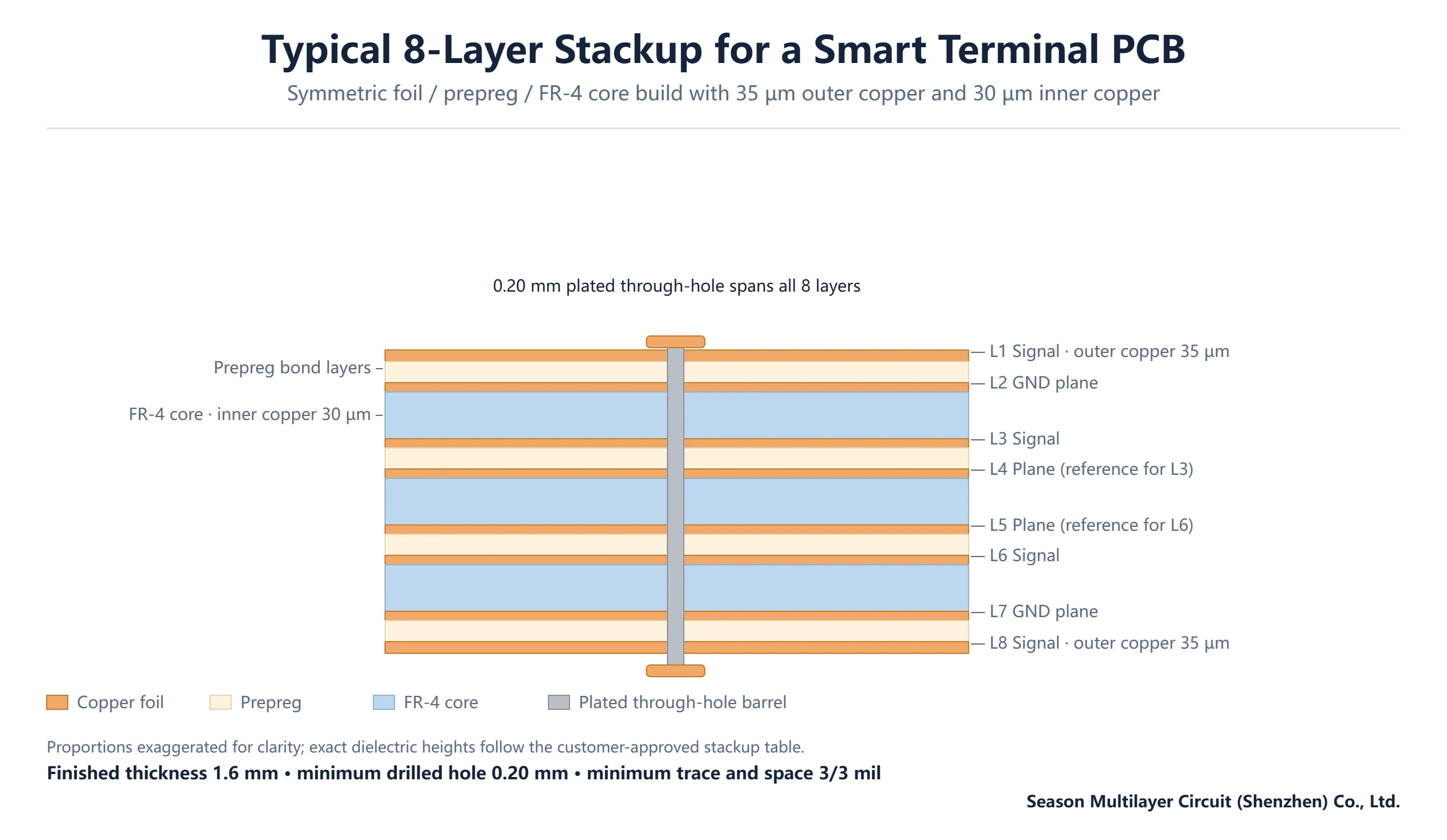
The stackup we use for this class of board is symmetric, with copper foil on the outer surfaces, prepreg bonding layers, and three FR-4 cores carrying the inner copper. From top to bottom the electrical assignment is: L1 signal, L2 ground, L3 signal, L4 plane, L5 plane, L6 signal, L7 ground, L8 signal. Every signal layer therefore has an adjacent, uninterrupted plane — L1 references L2, L3 references L4, L6 references L5, and L8 references L7.
The outer copper layers carry 35 µm (1 oz) of copper for current capacity on power entry and connector fanout, while inner layers carry 30 µm. The 0.20 mm minimum drilled via is a mechanically drilled plated through-hole that spans all eight layers, which keeps the build cost at standard multilayer level — no laser microvias are needed unless your design wants them. That distinction matters for budget: an HDI stackup with laser-drilled stages buys density but adds lamination cycles.
Symmetry is not cosmetic. Balanced copper and dielectric above and below the centerline keeps the board flat after lamination and reflow, which matters when the PCB is screwed into a thin plastic enclosure with standoffs at the corners. If you change one dielectric height during review, the mirror-side layer changes with it.
Wireless Coexistence: Layout Rules That Survive Certification
Most smart terminals fail certification not because the radio chip is bad, but because the board around it lets digital noise reach the antenna. The zoning discipline we apply on an 8-layer smart terminal PCB is simple to state and strict to follow: keep the RF section physically separated, keep digital return currents away from antenna feed paths, and give the power section its own island with bulk capacitance where the supply enters the board.
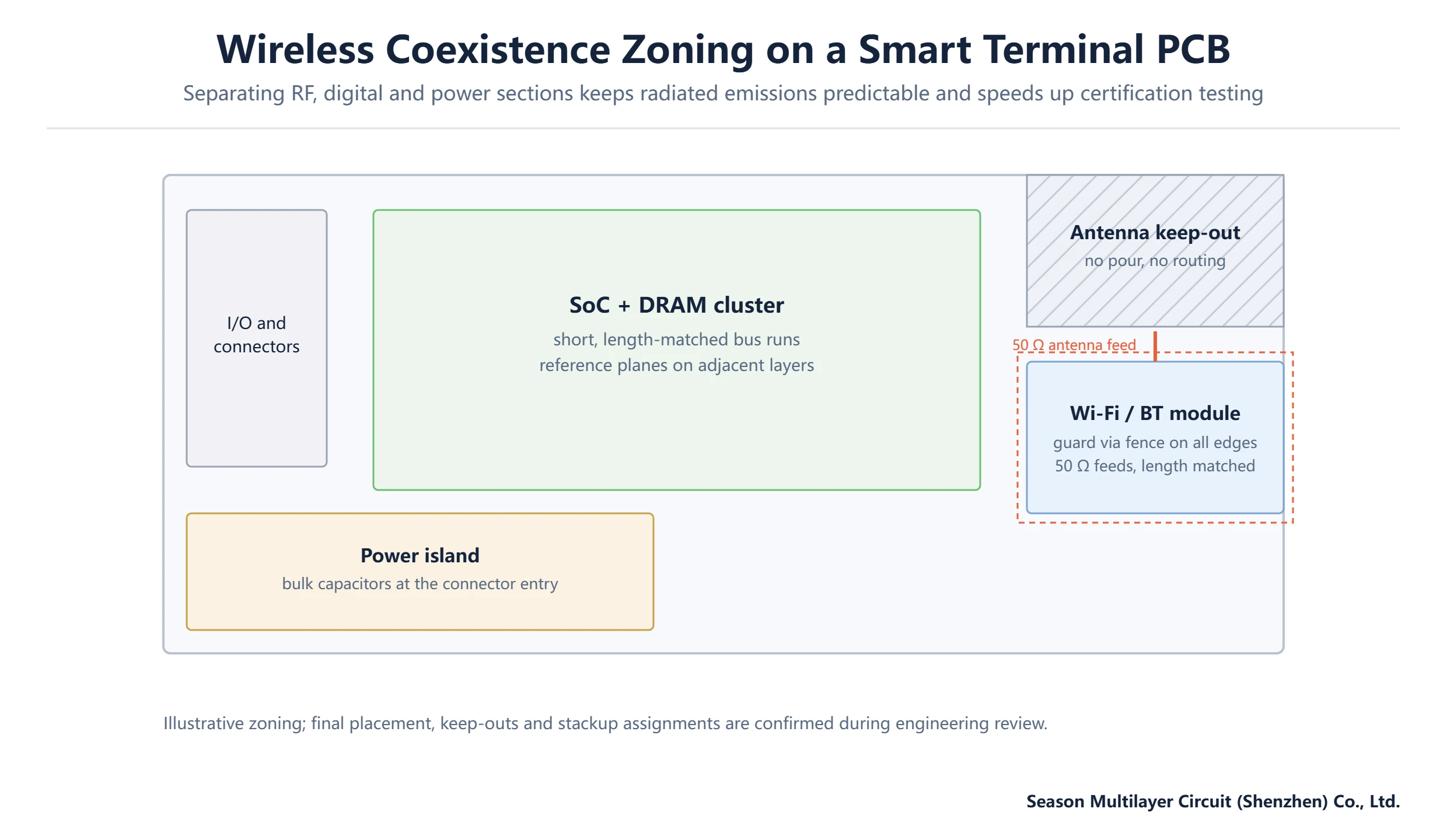
In practice this means the antenna keep-out occupies a board corner with no copper pour and no routing beneath it; the wireless module sits next to the keep-out, surrounded by a fence of stitched ground vias; the processor and memory cluster stays on the opposite side of the module fence with short, length-matched bus runs; and 50 Ω antenna feeds route on the outer layer over the L2 ground plane without crossing plane splits. Each of these rules is checkable in review, which is why boards zoned this way tend to pass radiated and conducted emissions on the first lab visit.
During DFM review we also look at the details that zoning diagrams do not show: guard via spacing along the module fence, the return path under every signal that crosses between zones, and crystal or switching-regulator placement relative to the antenna. If you are early in layout, send us the placement file rather than waiting for final Gerber data — moving a connector at layout stage costs an afternoon, moving it after fabrication costs a respin.
Choosing Between 2, 4, 6 and 8 Layers for a Terminal
Layer count is a trade between routing density, signal integrity and cost. The table below compares the classes we see in terminal products, expressed in relative terms. The cost multiplier for an eight-layer build against a comparable two-layer panel is roughly 1.6–2.2×, driven mostly by material and lamination cycles rather than labor.
| Dimension | 2-layer | 4-layer | 6–8 layer terminal build |
|---|---|---|---|
| Routing density | Low, single escape channel | Moderate | High, dual escape channels around fine-pitch BGAs |
| Reference planes | None | One full plane | Ground plane adjacent to every signal layer |
| RF capability | Uncontrolled | Basic 50 Ω runs | Controlled 50 Ω with keep-out zoning and via fencing |
| EMC behavior | Frequent rework iterations | Usually manageable | Predictable, certification-friendly |
| Relative fabrication cost | 1.0× | ≈1.3–1.5× | ≈1.6–2.2× |
The honest guidance: stay at four layers if your processor fanout fits and the product has no radio or only a coarse-positioning radio. Move to six when you need a full ground plane plus one high-speed bus layer. Move to eight when fine-pitch BGA escape, RF coexistence and a crowded connector edge all land on the same board — which is exactly the situation for most modern smart terminals. Our two-layer versus four-layer breakdown covers the lower end of that decision in detail.
BGA Fanout and High-Density Integration
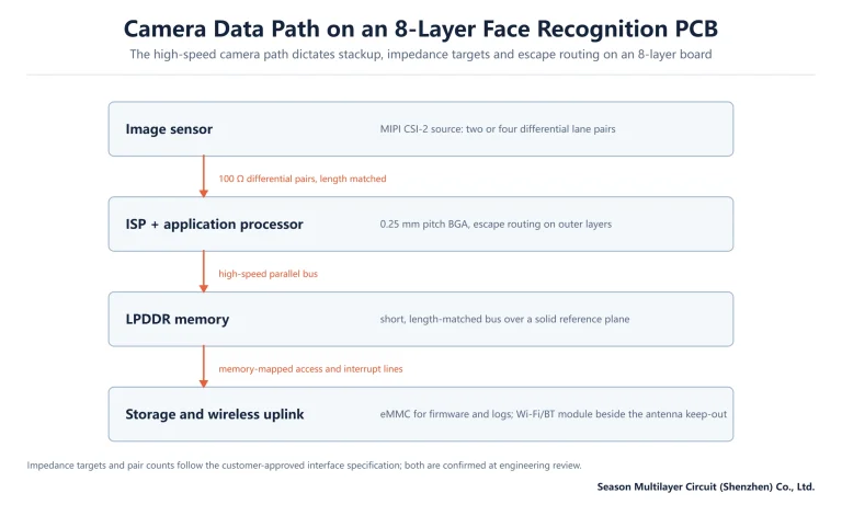
Terminal-class processors commonly land at 0.25 mm ball pitch, sometimes finer. At 0.25 mm pitch, a through-via lands between four balls and fans out on the layer directly beneath the device, which is why the stackup in the previous section reserves L1 and L3 for signal: the first escape channel runs under the outer pads, the second on L3 after the ground plane. With 3/3 mil trace and space, one escape channel per ball row is reliable without via-in-pad plating steps.
If your design pushes below 0.25 mm pitch or needs the balls directly on vias for thermal reasons, the conversation shifts from standard multilayer to HDI: laser-drilled microvias with 0.1 mm capability (down to 0.076 mm on reviewed builds), stacked or staggered, with resin plugging and capping where the via sits under a pad. That upgrade changes cost and lead time materially, so it should be a decision made at engineering review with the actual BGA map in hand — not a default. Memory is usually the easier part of the design: LPDDR buses tolerate moderate lengths but want length matching and a solid reference, both of which the symmetric stackup provides.
Manufacturing and Inspection Flow
Production for this build class runs the standard multilayer sequence — inner-layer imaging, lamination, drilling, plating, outer-layer imaging, solder mask, surface finish and legend — with inspection gates at the points where an eight-layer board can fail silently. Automated optical inspection covers every copper layer before lamination; after finish, 100% electrical test by flying probe or fixture confirms netlist continuity and isolation.
| Checkpoint | Method | What it protects |
|---|---|---|
| Inner-layer artwork | AOI before lamination | Catches trace shorts and opens while they are still repairable |
| Post-lamination registration | X-ray or coupon check | Confirms layer-to-layer alignment before drilling |
| Hole copper | First-article cross-section | Verifies plating thickness inside the 0.20 mm holes |
| Final netlist | 100% flying probe or ICT | Confirms every net matches Gerber data |
| Impedance | TDR on test coupon | Confirms 50 Ω RF and bus targets on the shipped build |
For terminal products we also see impedance verification used as a batch gate, not just a first-article event: the TDR coupon travels with each production lot, so a drift in the press cycle shows up before a customer assembly does. Acceptance criteria follow the IPC standards for bare-board workmanship, and certification copies of test reports ship with the goods on request.
Lead Time from Prototype to Volume
For this build class, prototype fabrication typically completes in 5–7 working days once engineering review is closed, and volume runs in the 15–20 working day range depending on quantity and laminate allocation. These windows assume the stackup is confirmed and no special-material allocation is pending; the binding schedule for your order is confirmed at engineering review, not at quotation.
Volume continuity is where the two-up panel and archived engineering parameters earn their keep. Because the same working files, panel program and inspection criteria are reused on repeat orders, boards from a later lot assemble the same as the first-article lot. Our production network — three plants across Shenzhen, Jiangxi and Anhui within the 998 PCB Group, founded in 2006, with 3,000,000 m² of annual capacity across 2–30 layer builds — absorbs demand peaks without changing the build recipe. For a sense of how a full order flows, the panel-to-shipment manufacturing walkthrough follows one build end to end.
What Actually Moves the Cost of an 8-Layer Terminal Board
Quotation for this class of board responds to a short list of levers, all of them relative rather than absolute. Layer count and finished size set the base; surface finish, minimum trace and space, and hole count adjust it; and panelization efficiency can move the unit price more than any of the technical parameters. A design that fits two boards on a 242 × 170 mm panel with room for test rails is measurably cheaper per board than the same circuit forced onto an awkward single-board panel.
- Base geometry: layer count, board outline and thickness class set the material and lamination baseline.
- Process floor: minimum trace and space (3/3 mil here, 2/2 mil capability for reviewed designs), minimum hole size and via count.
- Finish and mask: ENIG on this reference build; alternative finishes trade shelf life and assembly method differently.
- Panel efficiency: board size relative to the production panel, plus test fixture strategy.
- Order shape: prototype quantity versus repeat volume, and how far the repeat can reuse archived engineering parameters.
The practical takeaway is that the cheapest version of this board is the one whose constraints are declared early. When we know the BGA pitch, the RF zones and the connector field before quoting, the review optimizes panel and stackup once instead of respinning after a surprise.
Get Your Terminal Build Reviewed Before You Commit
If the reference build above is close to your design, the fastest next step is to submit your stackup intention and Gerber data for engineering review — we return feasibility comments on trace and space, via structure and panel efficiency, plus the production detail for the exact 8-layer intelligent terminal PCB build behind this article. If your design needs finer pitch or laser microvias, the review will say so with the cost and lead-time deltas attached, before you commit a layout.
Frequently Asked Questions
What files do I need to quote an 8-layer smart terminal PCB?
Gerber data including the drill files, plus your stackup intention (layer count, target thickness, copper weights) and any impedance requirements. If the design uses RF sections or fine-pitch BGAs, a placement file or a short note on the interface speeds helps the review give accurate feedback on the first pass.
How long does an 8-layer PCB prototype take?
For a standard through-via build like the reference specification here, prototype fabrication typically completes in 5–7 working days after engineering review is closed. Builds that add laser microvias or special laminates take longer because extra lamination cycles are involved. The binding date for your order is confirmed at engineering review.
Is an 8-layer PCB worth it compared with 6 layers for a smart terminal?
It depends on congestion and radio count. Six layers handle one high-speed bus plus a full ground plane well. When a fine-pitch BGA, a Wi-Fi/BT module and a crowded connector edge coexist, the extra pair of layers in an 8-layer smart terminal PCB gives each signal layer its own reference plane, which usually pays for itself in one avoided EMC rework cycle.
Which copper weight is used on smart terminal boards?
The reference build uses 35 µm (1 oz) outer copper and 30 µm inner copper, which suits the current levels of terminal-class devices. Heavier copper is available for power-focused designs, but on a consumer terminal it usually adds thickness and cost without benefit — the review confirms the carrying current your rails actually need.
How is wireless coexistence handled on the PCB?
Through zoning and stackup together: the antenna keep-out stays free of pour and routing, the module is fenced with ground vias, 50 Ω feeds run on an outer layer over an uninterrupted ground plane, and the power section is isolated with bulk capacitance at the entry point. These are review-checkable rules rather than style preferences.
What surface finish should I choose for a terminal board?
ENIG is the default on this build class because it stays flat and solderable through multiple assembly passes, which matters when both sides carry fine-pitch parts. Alternatives such as OSP or HASL suit simpler assemblies; the finish choice is confirmed during review based on your assembly process and shelf-life needs.
Will volume boards match the prototype quality?
Yes, because repeat orders reuse the same archived working files, panel program and inspection criteria as the confirmed prototype. First-article cross-sections and 100% electrical test run on production lots, and TDR impedance coupons travel with each batch so any process drift is caught before shipment.
Request an Engineering Review for Your Smart Terminal Board
Send your Gerber data and stackup intention, and our engineering team returns layout-level feedback on routing density, RF zoning and panel efficiency — typically the same working day. Quotation follows the review, itemized by the levers in this article, with no hidden line items.