Book Appointment Now

A buyer-side rigid flex PCB guide: structure, polyimide materials, manufacturing steps, design rules and relative cost logic, with supplier evaluation checks.
Rigid Flex PCB Explained: Structure, Manufacturing and Applications
When a product has no room for connectors but its electronics still need rigid support, the industry answer is a rigid flex PCB: rigid multilayer sections for components and power, joined without interruption by a polyimide flex core that folds into whatever space the enclosure leaves. One part replaces a rigid board, a flex tail, and the connectors and assembly labour between them – which is why camera modules, wearables and dense industrial controls specify it despite the premium. This guide explains the structure zone by zone, walks through the manufacturing process step by step, and then covers the side most articles skip: the design rules, relative cost logic and supplier checks that decide whether a rigid flex build succeeds at engineering review. All values are typical industry practice or our own production standards, confirmed per order before manufacturing.
Table of Contents
- What Is a Rigid Flex PCB?
- Rigid Flex vs a Flex-to-Board Assembly
- Structure: Rigid Zones, Flex Cores and Coverlay
- Materials: Polyimide, Adhesiveless Copper-Clad and Coverlay
- How a Rigid Flex PCB Is Manufactured
- Design Rules Buyers Should Confirm Early
- Rigid Flex PCB Applications Across Industries
- Cost Logic and Yield Challenges
- How to Evaluate a Rigid Flex Supplier
- FAQ
- Get Your Rigid Flex Stackup Reviewed
What Is a Rigid Flex PCB?
A rigid flex PCB is a single fabricated part that combines rigid multilayer sections and flexible circuit sections in one continuous laminate. The rigid zones carry components, connectors and copper planes much like any multilayer board; the flex zones are thin polyimide cores with copper that bend, fold and twist to connect the rigid zones electrically and mechanically. Because the whole structure is laminated as one piece, there are no soldered flex-to-board joints in the signal path.
That continuity is the defining property. In a conventional assembly, a rigid board connects to a separate flexible circuit through one or more connectors, and every connector adds contact resistance, assembly steps, and a failure point that vibrates, corrodes or works loose over time. A rigid flex circuit removes those interfaces entirely: the flex core is part of the board itself, so reliability problems shift from interconnect hardware to the laminate – where the fabricator, not the assembler, controls the outcome.
If you are new to how multilayer builds are named and bonded, the multilayer PCB explainer covers the fundamentals that rigid flex builds extend.
Rigid Flex vs a Flex-to-Board Assembly
The comparison that matters to a project is not rigid flex versus rigid – it is rigid flex versus rigid board plus separate flex plus connectors. The conventional approach looks cheaper per part, but the total bill includes connector hardware, flex assembly labour, extra procurement lines, and the field-failure rate of connector joints. Rigid flex moves that cost into fabrication, where it is paid once and covered by board-level testing.
| Factor | Rigid + flex + connectors | Rigid flex PCB |
|---|---|---|
| Signal path joints | Two solder joints per connector | None – one continuous laminate |
| Assembly steps | Board plus flex placement and soldering | Single part placement |
| Sourcing | Three suppliers to qualify and align | One fabricator owns the whole stackup |
| Failure modes | Connector wear, fretting, solder fatigue | Flex copper fatigue, controlled by bend radius design |
| Space and weight | Connector bodies add height and mass | Folds into the enclosure, minimal added height |
| Repair strategy | Connector replaceable | Rework is limited – design must be right up front |
The last row is the honest trade. A rigid flex PCB is harder to change after the fact, because the flex path is laminated, not plugged in. Projects accept that because the elimination of connectors buys back reliability that field service would otherwise have to supply.
Structure: Rigid Zones, Flex Cores and Coverlay
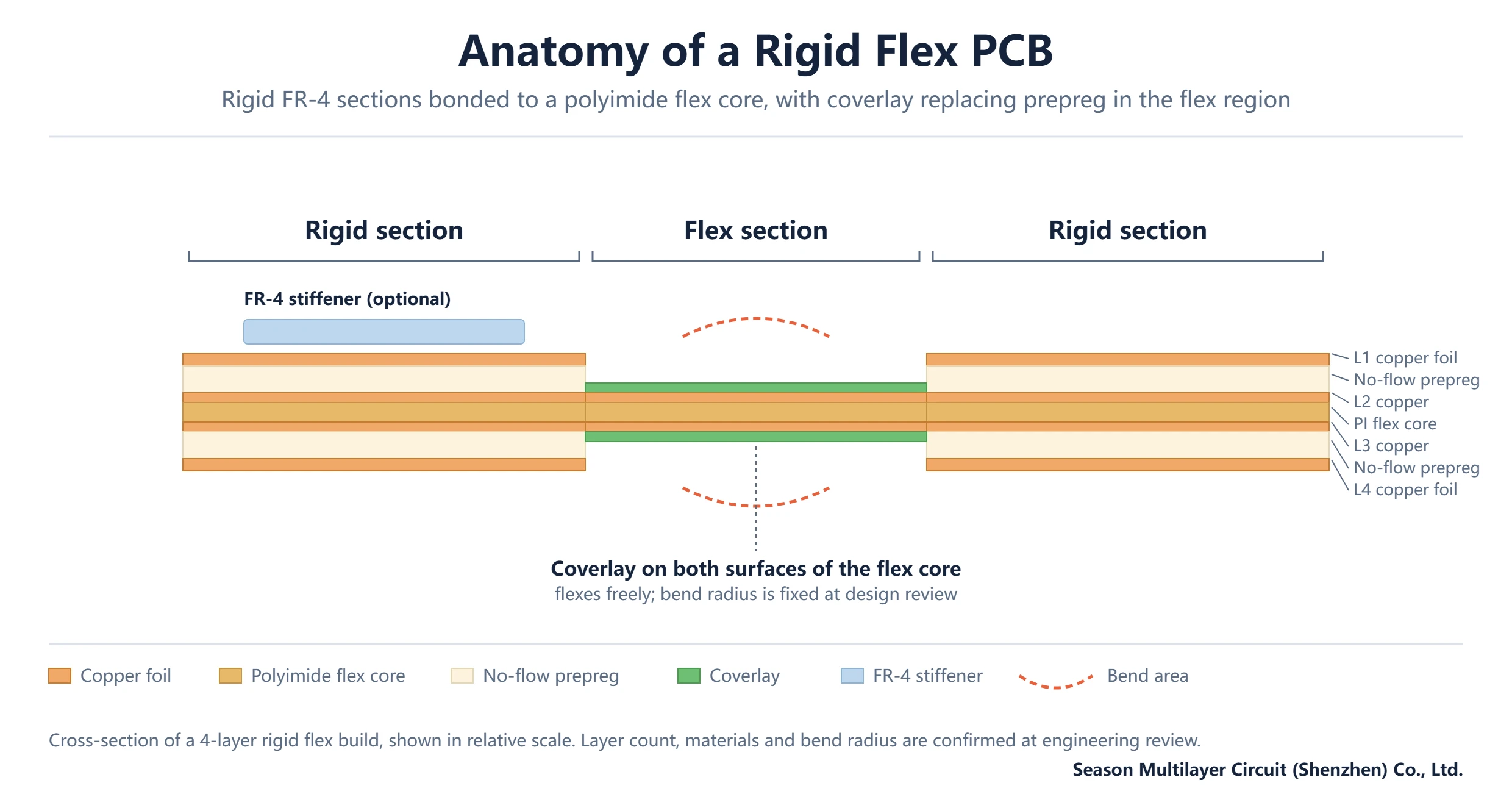
A rigid flex build is organised by zones. In the rigid sections, the stackup resembles a conventional multilayer: copper foils, no-flow prepreg bonds, and the flex core itself serving as an inner layer pair. In the flex section, everything unnecessary disappears – only the polyimide core, its two copper layers, and protective coverlay films remain, so the section stays thin enough to bend reliably. The transition between the two is where most of the manufacturing discipline lives.
| Zone | Typical construction | Role |
|---|---|---|
| Rigid section | Copper foil, no-flow prepreg, polyimide flex core, further copper layers; optional FR-4 stiffener | Components, planes, connectors, mechanical mounting |
| Transition | Gradual termination of rigid layers; coverlay steps in | Stress handoff between stiff and flexible regions |
| Flex section | Polyimide core with copper on both faces, coverlay on both surfaces | Bending interconnect between rigid zones |
| Bend area | Flex section only; neutral-axis copper placement | Dynamic or static folding per design radius |
Two details separate competent rigid flex work from the rest. First, copper in the bend area should sit on the neutral axis of the flex section – centered in the stack – so bending stretches neither surface excessively. Second, the transition zone should avoid abrupt stiffness steps right at component edges, where solder joints see the most bending stress. Both are design-review items, not production accidents to be fixed later.
Materials: Polyimide, Adhesiveless Copper-Clad and Coverlay
Material selection in rigid flex is dominated by the flex core. Adhesiveless copper-clad polyimide – copper bonded directly to polyimide without an adhesive layer – is the standard for anything that bends, because adhesive layers creep under repeated flexing and add thickness that works against tight bend radii. The polyimide core keeps its mechanical properties across a wide temperature range, which is why it survives lamination temperatures that would degrade adhesive-based constructions.
The rigid sections use conventional laminate systems, but with no-flow or low-flow prepreg so the resin does not squeeze into the flex zone during lamination. Coverlay – a polyimide film with adhesive, pierced with openings for pads – protects the flex copper the way solder mask protects rigid circuits, while staying flexible. FR-4 stiffeners are bonded where connectors or zero-insertion-force edges need local rigidity inside a nominally flexible region.
Laminate and coverlay systems are qualified under recognition programs run by UL Solutions, so the material stack chosen at review also determines the recognition marks the finished part can carry. Confirm materials by grade name in the fabrication drawing – substitutions change bend performance and certification together.
How a Rigid Flex PCB Is Manufactured
Rigid flex manufacturing combines the flex circuit process and the multilayer rigid process into one sequential flow. The sequence below is the standard pattern; each fabricator arranges the middle steps around its own equipment set.
- Design and stackup review: the flex path, bend radius and transition zones are checked against process capability before quoting, and Gerber data is validated at CAM.
- CAM engineering: panelisation, flex nest orientation, and compensation for material movement are planned; fabrication and stiffener drawings are confirmed with the customer.
- Flex core processing: the polyimide cores are imaged, etched and coverlay-laminated while still in panel form.
- Rigid layer processing: conventional inner layers are imaged and etched for the rigid sections.
- Lamination: rigid layers, no-flow prepreg and flex cores are pressed into one laminate, with pressure and temperature profiles tuned so resin does not invade the flex zone.
- Drilling and plating: through-holes are drilled through the rigid sections and plated; holes in or near flex zones get extra attention at review.
- Outer layer imaging, etching and surface finish, followed by coverlay opening exposure where the flex sections terminate.
- Electrical test, AOI and dimensional checks, with flex-zone bend samples pulled from production panels per the inspection plan.
Lamination is the step where rigid flex earns its price tag: every press cycle must hold the rigid layers in registration without damaging the flex cores, and the no-flow prepreg window is narrower than in conventional multilayer work. Our PCB lamination process walkthrough explains the base process that this sequence extends. Design data interchange follows the standard Gerber format maintained by Ucamco, with the flex outline and bend lines documented in the fabrication drawing.
Design Rules Buyers Should Confirm Early
Bend radius is the first number to fix. As standard industry guidance for flex circuits, a static bend – folded once during assembly – wants a radius of roughly ten times the flex thickness, while a dynamic bend that flexes in service wants far more headroom, commonly a hundred times or a rolling-flex design. The exact figure depends on copper weight, the number of flex layers, and whether the design is one- or double-sided flex, and it is confirmed at engineering review against IPC-2223 design practice, which is maintained through the standards catalog of the Global Electronics Association.
Transition zones deserve the second look. Traces crossing from rigid into flex should run perpendicular to the bend axis, without width steps or vias inside the transition, so bending stress spreads evenly instead of concentrating at an edge. Pads should be anchored with teardrops or fillets where traces leave the flex zone, and grain direction of the rolled-annealed copper should follow the bend axis so the copper works with the fold rather than against it.
Finally, dimension the flex path in its flat state and specify the folded form separately. Fabricators inspect the flat panel; the enclosure sees the folded result. When the two are not reconciled in the drawing, the mismatch surfaces as an assembly-line fit problem – discovered at the worst possible time.
Rigid Flex PCB Applications Across Industries
Camera modules are the canonical case: the image sensor sits on a rigid island, and the flex tail folds into a body that has no vertical space for a connector stack. Wearables follow the same logic – a children’s smartwatch build, for example, packs a six-layer HDI stackup behind the display and folds its interconnect to fit a curved housing, as described in our kids smartwatch PCB stackup guide. Anywhere the enclosure curves around the electronics, rigid flex removes the assembly compromises.
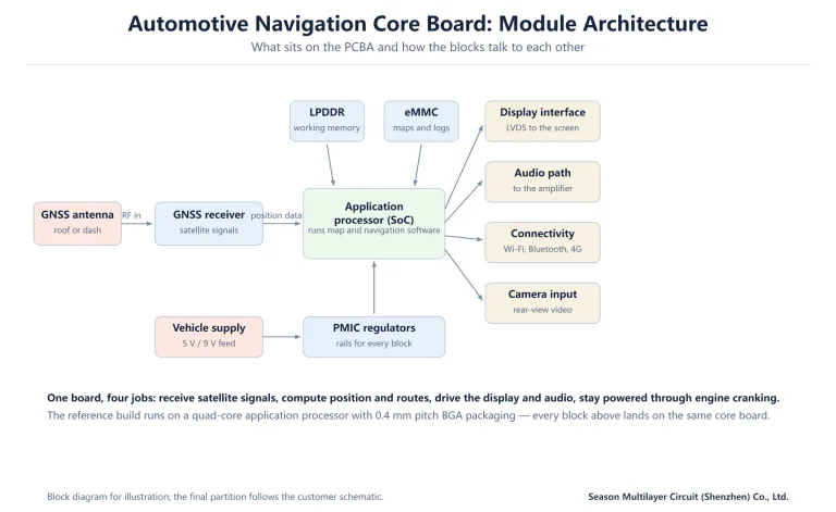
Communication and computing hardware use rigid flex to eliminate interconnect across vibrating or frequently mated regions, and industrial equipment uses it where cable harnesses would otherwise age. Automotive interiors and sensor clusters are a growing share: the vibration environment punishes connectors, so folding the interconnect into the board itself is a reliability decision as much as a packaging one. Core-board style builds follow the same pattern, as our automotive navigation core board PCBA example shows.
The common thread across all of these applications is not flexibility for its own sake – it is the elimination of a connector that the product could not afford, mechanically or spatially. That framing also tells you when not to use rigid flex: if a connector is genuinely fine, the conventional build is cheaper and easier to service.
Cost Logic and Yield Challenges
Rigid flex carries a premium over equivalent rigid multilayer work, and the premium is structural rather than arbitrary. Materials cost more – adhesiveless polyimide cores and coverlay price well above FR-4 laminates. Process steps multiply: flex and rigid layers are processed separately before lamination, lamination itself is more delicate, and inspection covers both regimes. As a planning range, a rigid flex build commonly prices at several times a comparable all-rigid multilayer panel, with the multiple narrowing at volume.
| Cost driver | Direction | Why |
|---|---|---|
| Flex core count | More layers, higher cost | Each polyimide core adds processing and lamination complexity |
| Bend count and tightness | Tighter bends, higher cost | Thinner cores, more coverlay steps, tighter process control |
| Rigid-to-flex ratio | More rigid area, lower relative cost | Rigid processing is cheaper per layer than flex handling |
| Panel utilisation | Better nesting, lower unit cost | Flex shapes waste panel area if nested poorly |
| Volume | Higher volume, lower unit cost | Setup and engineering-review effort amortises |
Yield is the second half of the cost story. The flex sections cannot be touched by many of the automated handling steps rigid panels rely on, and a defect in a laminated flex path usually condemns the whole part rather than a single layer. Experienced fabricators manage this with panel-level process control and conservative design-rule enforcement at review – which is why a fabricator that quotes rigid flex without questioning your bend radius is a warning sign, not a convenience.
How to Evaluate a Rigid Flex Supplier
Supplier evaluation for rigid flex starts with one question: how much of the flex process does the factory own in-house? A supplier that laminates, images and coverlays flex cores on its own floor controls the failure modes directly; one that outsources the flex cores inspects what it cannot control. Layer capability in the 4-to-16-layer range, including HDI constructions on rigid flex, should be demonstrated with reference builds rather than claimed on a website – our 6-layer rigid flex PCB page documents one production example.
Second, ask what the engineering review covers. A serious review challenges the bend radius, the transition-zone trace routing, stiffener placement and the flat-versus-folded dimensioning before quoting – the issues that become field failures later. Third, confirm the inspection package: electrical test, AOI, and bend or coupon samples from production panels, with acceptance to IPC Class 2 or Class 3 as the order requires. Our production campus runs flex and rigid processes on the same site, as the facility aerial view and the capability pages describe.

One practical final check: request the failure-mode discussion, not just the capability list. A supplier who can explain how their process catches coverlay alignment drift, resin invasion at transitions and copper fatigue at bends is telling you they have paid for those lessons already. That conversation is worth more than any datasheet.
Frequently Asked Questions
What is a rigid flex PCB?
A rigid flex PCB is a single laminated part that combines rigid multilayer sections with flexible polyimide sections. The rigid zones carry components and planes; the flex zones fold to connect them, replacing the separate flex circuit, connectors and solder joints of a conventional assembly with one continuous interconnect.
How many layers can a rigid flex PCB have?
Practical builds range from 4 to 16 layers, with the flex core pair counting as inner layers of the stackup. Higher-layer and HDI-style rigid flex constructions are quoted per design after engineering review, because lamination complexity and registration demands grow with every added layer.
What materials are used in a rigid flex PCB?
The flex core is adhesiveless copper-clad polyimide, protected by polyimide coverlay film. Rigid sections use conventional laminate with no-flow prepreg so resin does not invade the flex zone, plus optional FR-4 stiffeners where connectors need local rigidity. Material grades are confirmed by name at engineering review because they set both bend performance and certification.
How much does a rigid flex PCB cost compared with a rigid board?
As a planning figure, rigid flex commonly prices at several times a comparable all-rigid multilayer panel, driven by polyimide materials, separate flex processing, and more delicate lamination and inspection. The premium narrows at volume, and against the full bill of a rigid-plus-flex-plus-connector assembly the gap can be smaller than it first appears.
What is the minimum bend radius for a rigid flex PCB?
Standard industry guidance is roughly ten times the flex thickness for a static bend folded once during assembly, and a hundred times or a rolling-flex design for dynamic flexing in service. The exact radius depends on copper weight and flex layer count and is confirmed at engineering review against IPC-2223 design practice.
Where are rigid flex PCBs used?
Camera modules, wearables, communication hardware, industrial controls and automotive interior electronics are the main users. The common factor is a connector that the product could not afford: rigid flex removes it by folding the interconnect into the laminate itself, saving height, weight and a field-failure point.
How long does rigid flex prototyping take?
Expect a longer schedule than an equivalent rigid multilayer prototype, because flex cores are processed separately and lamination is more involved. A typical range is two to three weeks depending on layer count and material availability, with the exact date confirmed at engineering review against the production calendar.
Get Your Rigid Flex Stackup Reviewed
Submit your Gerber data, bend requirements and enclosure constraints, and the engineering team will review the rigid flex trade on your actual design – stackup, bend radius, transition zones and stiffener placement – and return a manufacturable recommendation with relative cost logic. Start through our PCB manufacturing services page; design data stays confidential and is used only for the review.