Book Appointment Now

Why ENIG PCB solderability fails at assembly, how black pad forms under intact gold, and the process windows and incoming tests that catch weak panels early.
ENIG PCB Solderability Failures: Black Pad, Dewetting and Fixes
A board that passes flying-probe and AOI can still turn into scrap the moment it hits the reflow oven. When ENIG pads refuse to wet, wet only in patches, or form dull grainy joints, the failure usually traces back to the plating line rather than the assembly floor — and by then the panel has already absorbed your component and assembly cost. ENIG PCB solderability problems are among the most expensive defects in electronics because they surface at the very last step of the chain.
This guide explains how electroless nickel immersion gold actually works, why its most common failure modes — black pad, dewetting and non-wetting — develop under visually intact gold, and which process parameters and incoming tests separate a disciplined finish line from a marginal one. If you specify ENIG in your RFQ, this is the checklist to negotiate against.
Table of Contents
- What ENIG Deposits on Copper (and Why It Solders Well)
- ENIG PCB Solderability Defects and Their Signatures
- Black Pad Corrosion: The Hidden Failure Under Intact Gold
- Nickel Bath Chemistry Drift: Concentration, pH and Temperature
- Copper Preparation and Microetch Control
- Rinsing, Drying and ENIG PCB Solderability in Storage
- Paste Selection and Reflow Window on Nickel-Gold Pads
- Incoming Tests That Catch ENIG PCB Solderability Risk
- A Process Control Window You Can Ask Suppliers For
- How to Specify ENIG in Your RFQ
- Have Your ENIG Finish Reviewed Before You Commit
- FAQ
- Get Your ENIG Stackup and Finish Reviewed
What ENIG Deposits on Copper (and Why It Solders Well)
ENIG builds two layers over the copper pad. First, an autocatalytic electroless nickel layer — typically 3–6 µm — provides the solderable metal and a diffusion barrier against copper. Second, a thin immersion gold layer, typically 0.05–0.1 µm, protects the nickel from oxidation. The gold exists only as a protective skin; it dissolves into the solder joint during reflow, and the actual metallic bond forms between molten solder and the nickel surface as an intermetallic layer (Ni₃Sn₄ on SAC alloys).
That structure explains both the appeal and the risk. Because the pad surface is planar, ENIG suits fine-pitch BGA, QFN and 0.4 mm-pitch components where HASL domes would interfere. Because the solderable surface is nickel, however, the quality of the joint depends on nickel deposition chemistry — a wet chemical process with narrow windows — rather than on the gold you can see. A bright, gold-looking pad can still be unsolderable underneath.
For a broader comparison of nickel-based finishes, see our ENEPIG surface finish guide, which adds a palladium layer between nickel and gold to address some of the mechanisms described below.
ENIG PCB Solderability Defects and Their Signatures
Wetting failures on nickel-gold pads are not one defect but a family of them, and each has a different root cause. Reading the failure signature correctly is half the diagnosis: the same symptom of “solder did not stick” can point to bath chemistry, to copper preparation, or to storage and handling.
| Defect seen at assembly | Typical signature | First thing to check |
|---|---|---|
| Non-wetting | Solder balls up and rolls off; pad stays exposed and grey | Nickel surface contamination or passivation — check storage and rinse data |
| Dewetting | Solder wets first, then retracts into mounds with thin patches | Nickel layer too thin or porous; copper diffusion through the nickel |
| Black pad | Joint separates cleanly at pad; dark nickel surface under the lifted solder | Hyper-corrosive nickel bath; grain-boundary attack during gold immersion |
| Dull or grainy joints | Joint forms but looks rough, voids concentrate at the interface | Nickel crystallization drift — bath temperature or pH out of window |
| Pad discoloration before assembly | Gold looks blotchy, brownish or stained | Insufficient final rinse; dried chemistry residue on the pad |
Two of these signatures deserve special attention. Dewetting usually means the nickel barrier failed to stop copper migration — the copper oxidized at the surface during the dwell between finishing and assembly. Black pad is the opposite: the nickel was corroded during plating itself, so the damage was built into the panel on the production floor.
Black Pad Corrosion: The Hidden Failure Under Intact Gold
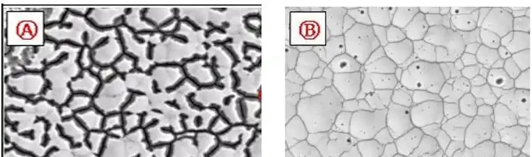
Black pad is the best-known ENIG failure and the hardest to see, because the gold layer that faces you is decorative, not structural. During immersion gold plating, the displacement reaction consumes nickel atoms at the surface. If the nickel bath leaves a rough, columnar or over-phosphorus microstructure, the gold displacement attacks along grain boundaries and leaves a corroded, phosphorus-rich nickel layer underneath a visually perfect gold film.
At reflow, solder meets that corroded layer instead of sound nickel. The wetting may look acceptable, but the intermetallic cannot anchor, so the joint shears off the pad with little or no solder residue — the classic “clean lift” that fails cross-section review or shows up as an intermittent field failure. SEM inspection of a black pad surface shows the mud-crack or grain-boundary morphology that ordinary optical inspection misses entirely.
Because the mechanism lives in nickel deposition chemistry, prevention is a plating-line discipline issue: bath analysis on a fixed schedule, controlled withdrawal of the immersion gold step, and cross-section coupons pulled per bath campaign. A supplier who cannot show you nickel grain micrographs should not be quoting BGA-heavy ENIG work.
Nickel Bath Chemistry Drift: Concentration, pH and Temperature
The electroless nickel bath is a balance of nickel salt, reducing agent, complexing agents and stabilizers. Nickel concentration pushed too high accelerates deposition and produces a porous, sponge-like layer that copper diffuses through and that gold displaces unevenly. Concentration run too low starves the pad — below roughly 3 µm of nickel the copper barrier is marginal, and dewetting follows. Complexing agent depletion causes uneven deposition and local hyper-corrosion, which is one of the direct precursors of black pad.
pH and temperature amplify every other drift. The operating window for most chemistries sits between pH 4.6 and 5.2; below about 4.0 deposits turn dark and brittle, above about 5.5 the solution hydrolyzes and precipitates. Temperature is usually specified at 85–90 °C, and swings beyond roughly ±2 °C coarsen the nickel crystallization — measurably degrading wetting. Metallic contaminants such as iron or copper ions in the bath co-deposit into the layer and create the same porosity as an over-accelerated bath.
None of this is visible on the finished panel, which is exactly why bath analytics belong in your supplier conversation. The control table later in this article lists the parameters worth asking for in a monthly process report.
Copper Preparation and Microetch Control
Before nickel can deposit, the exposed copper must be chemically clean and properly roughened. Residual copper oxide — a film thicker than roughly 5 nm is enough — blocks the nickel-to-copper bond and produces adhesion well below the ~12 N/cm class expected of a sound interface. Organic films are just as damaging: fingerprint oils and mold-release residue create local no-deposit zones that later read as non-wetting pads.
Microetch depth has a narrow optimum. Under-etched copper (average roughness below roughly 0.3 µm Ra) leaves the nickel weakly anchored, and the interface begins to separate after repeated thermal excursions. Over-etched copper (above roughly 0.8 µm Ra) presents an irregular surface that the electroless nickel covers unevenly, seeding micro-cracks in the deposit. Either extreme shortens the working life of the joint, so etch rate is tracked by copper weight loss on witness coupons, not by visual appearance.
Plasma cleaning is sometimes used on high-reliability builds to strip organic contamination before wet processing, and anti-tarnish dips protect the copper between microetch and nickel strike. These are the steps that never appear on a data sheet but show up immediately in wetting balance numbers.
Rinsing, Drying and ENIG PCB Solderability in Storage
Post-plating rinsing is where a sound finish is most often ruined. Residual plating salts left on the pad — rinse water conductivity above roughly 10 µS/cm is a red flag — react with flux and moisture during storage and assembly. Sulfide residues are particularly aggressive: they form compounds with the tin in the solder that raise the contact angle above the ~35° ceiling that good wetting requires. Multi-stage counterflow rinsing with deionized water, followed by hot-air or vacuum drying, is the standard defense.
Storage drift is quieter but just as real. In environments above roughly 60% relative humidity, the gold surface adsorbs moisture and the underlying nickel slowly forms a hydroxide passivation layer that can depress solderability measurably within a few days of exposure. Vacuum-sealed packaging with desiccant, and a defined shelf-life policy confirmed at engineering review, keep the finish in as-plated condition. Boards pulled from a humid warehouse and reflowed without baking are a classic false alarm — the finish gets blamed for a logistics problem.
The practical guidance: treat ENIG panels like a perishable commodity. Keep them sealed, dry and out of direct handling until loading, and require your assembler to wear gloves — skin oils on a gold pad behave like a mask during reflow.
Paste Selection and Reflow Window on Nickel-Gold Pads
Even a well-plated panel can fail at assembly if the paste and profile do not match the finish. Nickel oxide is more tenacious than the oxides on bare copper, so flux activity matters: no-clean ROL0-class fluxes sometimes lack the acidity to strip a slightly passivated nickel surface, while ROL1-class or halide-activated formulations restore margin. The trade-off is residue corrosivity, which brings us back to cleanliness testing on the assembly side.
Powder size should follow pad geometry. For fine-pitch pads below 0.4 mm pitch, Type 4 powder (20–38 µm) reduces bridging and improves paste release from the stencil. The profile matters as much as the chemistry: a preheat ramp steeper than roughly 3 °C/s evaporates flux solvents before they can activate, cutting wetting force measurably. SAC alloys need peak temperatures of about 245 °C or higher to grow a continuous Ni₃Sn₄ intermetallic; a short peak leaves a patchy interface that shears under vibration.
For tight-pitch BGA work on ENIG, the assembly window is best validated on your own product with a wetting balance or dross-and-flow check on real coupons, not on the supplier’s test vehicle. Our SMT assembly process guide covers the profile and stencil decisions that pair with nickel-finish boards.
Incoming Tests That Catch ENIG PCB Solderability Risk
Every mechanism described above leaves evidence that a buyer can demand before committing components. The cheapest screen is thickness: X-ray fluorescence (XRF) measurement of the gold and nickel layers takes seconds per pad and immediately exposes thin-nickel or heavy-gold baths. Wetting balance testing to the solderability requirements of IPC solderability standards turns chemistry into a number — time-to-wet under a fixed flux — while a simple contact-angle reading catches gross passivation without any lab work.
| Incoming test | Method reference | What it tells you | Typical acceptance |
|---|---|---|---|
| XRF thickness survey | XRF per IPC-4552 guidance | Gold and nickel thickness across the panel | Nickel 3–6 µm; gold 0.05–0.1 µm |
| Wetting balance | Solderability test methods | Time to wet on nickel surface with production-matched flux | Wetting within a few seconds; no dewetting on withdrawal |
| Contact angle check | Simple sessile-drop reading | Gross organic passivation or residue on pads | Well below ~35° on freshly fluxed pads |
| Cross-section with SEM | Metallographic coupon review | Nickel grain structure, phosphorus layers, interfacial corrosion | No grain-boundary attack; continuous intermetallic after reflow |
| Ionic cleanliness | ROSE or ion chromatography | Rinse quality and residue risk on finished panels | Below the level agreed with your assembler’s flux system |
Cross-sectioning is the decisive test because it sees what XRF cannot: the nickel microstructure and any grain-boundary corrosion. A supplier confident in its bath discipline will pull coupons per production run and share micrographs; one that resists is telling you something. Our incoming inspection guide covers the material side of the same receiving routine.
A Process Control Window You Can Ask Suppliers For
The parameters below compress the mechanisms in this article into a control table. None of them is exotic; each is logged by a competent finishing line as a matter of routine. Asking a prospective supplier to state their windows — and their reaction when a parameter drifts — is a fast way to separate disciplined ENIG capability from a process that occasionally surprises its customers.
| Parameter | Typical control window | What drift causes |
|---|---|---|
| Nickel bath pH | 4.6–5.2, auto-dosed | Dark brittle deposits below window; hydrolysis and precipitate above |
| Nickel bath temperature | 85–90 °C, ±2 °C | Coarse crystallization and depressed wetting outside band |
| Nickel thickness | 3–6 µm per IPC-4552 class | Copper diffusion and dewetting when thin; brittle joints when excessive |
| Gold thickness | 0.05–0.1 µm | Exposure and passivation of nickel when thin; embrittlement risk when heavy |
| Microetch rate | Tracked by copper weight loss | Weak adhesion under-etched; micro-cracked deposit over-etched |
| Final rinse resistivity | DI water, multi-stage | Salt residues, sulfide formation, raised contact angle |
| Packaging | Vacuum seal with desiccant | Hydroxide passivation of nickel in humid storage |
Two practices separate good lines from average ones. First, bath analysis on a fixed schedule with recorded corrective actions, rather than chemistry maintained only when a failure appears. Second, coupon-based process control: a test coupon through every bath campaign, cross-sectioned at defined intervals, with the micrographs retained. A line that already runs these steps will answer your questions without a meeting.
How to Specify ENIG in Your RFQ
Most ENIG surprises start with a one-line RFQ: “surface finish: ENIG.” The specification leaves every decision that governs solderability to the supplier. A stronger RFQ pins the parameters that matter for your assembly and asks for evidence that the line holds them. The items below cost nothing to request and take an hour to negotiate once.
- State nickel and gold thickness targets (for example, nickel 3–6 µm, gold 0.05–0.1 µm) and require XRF data per panel lot.
- Ask for the bath control windows for pH, temperature and contaminant levels, and how often chemistry is analyzed.
- Require cross-section coupons per campaign on BGA-dense designs, with SEM review available on request.
- Specify packaging (vacuum seal, desiccant) and the shelf-life position the supplier will honor.
- Agree in advance which solderability test and flux will be used to arbitrate a dispute, so both sides measure the same way.
If your design carries fine-pitch BGAs, rework-heavy positions, or long warehouse dwells, also read our plating voids guide — voided microvias under ENIG pads create their own wetting and reliability symptoms that no surface finish test will catch. For mixed-technology builds, ENEPIG is often worth the premium for exactly these reasons.
Have Your ENIG Finish Reviewed Before You Commit
Season Multilayer Circuit supports ENIG, ENEPIG, HASL and OSP finishes across 2–30 layer boards, with bath analytics and coupon-based process control on every ENIG campaign. Submit your Gerber data and assembly requirements through our PCB manufacturing services page and our engineering team will confirm finish thickness targets, coupon policy and packaging before production — so solderability is engineered in, not inspected in.
Frequently Asked Questions
What causes black pad on ENIG PCBs?
Black pad starts in the electroless nickel bath. A rough or over-phosphorus nickel microstructure lets the immersion gold displacement reaction attack along grain boundaries, leaving a corroded, phosphorus-rich layer under visually intact gold. Solder cannot anchor to that layer, so joints lift cleanly at the pad during assembly or thermal cycling.
What nickel and gold thickness should ENIG have for good solderability?
Industry guidance for ENIG calls for a nickel layer of roughly 3–6 µm with a gold layer of 0.05–0.1 µm. Nickel below about 3 µm gives marginal copper diffusion protection and invites dewetting; gold far above the range adds cost and can contribute to brittle intermetallic formation in the joint.
How can I detect ENIG solderability problems before assembly?
Combine XRF thickness surveys on received panels, a wetting balance or contact-angle check with a production-matched flux, and — for BGA-dense designs — cross-section review of supplier coupons. SEM inspection of the nickel surface is the only way to confirm the absence of grain-boundary corrosion that optical checks miss.
Does storage time affect ENIG solderability?
Yes, mainly through humidity. Above roughly 60% relative humidity, moisture uptake promotes a nickel hydroxide passivation layer under the gold that measurably depresses wetting within days. Vacuum-sealed packaging with desiccant, dry warehouse conditions and a defined shelf life keep the finish in as-plated state.
Is ENEPIG better than ENIG for solderability?
ENEPIG adds a palladium layer between nickel and gold, which stops the galvanic displacement attack that produces black pad and gives a more stable solderable surface across multiple reflows and wire-bonding steps. It costs more, so many buyers specify ENIG for standard builds and ENEPIG for fine-pitch, high-reliability or mixed bonding applications.
What reflow peak temperature should I use on ENIG pads?
For SAC lead-free alloys, plan on a peak of about 245 °C or higher so the Ni₃Sn₄ intermetallic grows continuously across the pad. Keep the preheat ramp below roughly 3 °C/s so flux solvents survive to activation, and match flux activity (ROL1-class or stronger) to the actual nickel surface condition.
Can ENIG solderability issues be repaired after delivery?
Not reliably at the pad level. Mild passivation can sometimes be recovered with an appropriate flux and re-bake, but black pad corrosion and interfacial contamination are built into the finish and cannot be removed without re-plating. That is why prevention at the plating line and incoming verification are the only economic controls.
Get Your ENIG Stackup and Finish Reviewed
Send your Gerber files and component plan to Season Multilayer Circuit, and our engineers will review pad geometry, finish thickness and coupon policy against your assembly process before quoting. Start at the manufacturing services page or browse our finished boards, such as this 8-layer security system PCB, to see the ENIG builds we ship weekly.