Book Appointment Now

A buyer-side guide to the ENEPIG surface finish: layer stack and thicknesses, black pad prevention versus ENIG, wire bonding, cost logic and use cases.
ENEPIG Surface Finish: Pros, Cons and When to Specify It

You specified ENIG for years and it mostly worked — until a batch of BGA pads came back with the dull, corroded nickel patch your assembler calls black pad. Or your next design needs gold wire bonding that ENIG’s ultra-thin gold, sitting directly on nickel, cannot reliably support. These are exactly the two problems the ENEPIG surface finish was developed to solve, and they explain why it has become the default choice for automotive control boards, gold-wire-bonded modules and high-insertion connector hardware.
This guide explains how each layer of the Ni-Pd-Au stack works, where ENEPIG genuinely outperforms ENIG and full-body gold plating, what drives its cost in relative terms, and how to specify it on a fabrication drawing so quotes come back comparable. The emphasis throughout is on decisions a hardware engineer or procurement team can act on — not on plating chemistry for its own sake.
Table of Contents
- What Is the ENEPIG Surface Finish?
- The ENEPIG Layer Stack: What Each Metal Does
- ENIG vs ENEPIG: How the Palladium Layer Kills Black Pad
- Wire Bonding, Reflow and Assembly Behavior
- Contact Durability: Connectors, Edge Fingers and Insertion Cycles
- ENEPIG Cost Logic: Where the Money Actually Goes
- Process Control: What Your Fabricator Must Hold Steady
- Where ENEPIG Fits: A Selection Table
- How to Specify an ENEPIG Surface Finish on Your Fab Drawing
- ENEPIG Surface Finish: Key Takeaways
- FAQ
- Get Your Surface Finish Reviewed Before You Order
What Is the ENEPIG Surface Finish?
ENEPIG stands for Electroless Nickel, Electroless Palladium, Immersion Gold — three metallic layers grown chemically, one after another, on every exposed copper feature of the board. Because all three layers deposit by autocatalytic or exchange chemistry rather than by electric current, coverage is uniform even inside via openings, on via walls, and across dense fine-pitch pads where electroplating struggles to distribute current evenly.
The deposit sequence matters. First an electroless nickel layer (typically 3–6 µm) provides the diffusion barrier and the mechanical base. Then a thin electroless palladium layer (typically 0.05–0.15 µm) is grown on top of the nickel. Finally an immersion gold flash (typically 0.03–0.08 µm) protects both metals underneath. The finish is standardized under IPC-4556, one of the surface-finish specifications maintained by the IPC standards family now overseen by the Global Electronics Association.
For a buyer, the practical appeal is consolidation: a single finish that must solder reliably, tolerate several reflow cycles, accept gold wire bonds, and survive repeated contact insertion — without the black-pad failure mode that haunts ENIG and without the cost of full-area electrolytic gold.
The ENEPIG Layer Stack: What Each Metal Does
Each layer in the stack has a distinct job, and removing any one of them breaks the finish’s logic. Nickel is the structural and diffusion barrier; palladium is the corrosion barrier and the wire-bondable layer; gold is the protective, solderable skin. The table below summarizes the roles and the thickness ranges commonly quoted in industry practice.
| Layer | Typical thickness | Function in the stack |
|---|---|---|
| Immersion gold | 0.03–0.08 µm | Solderable, oxidation-resistant skin; protects the palladium and nickel beneath from tarnish |
| Electroless palladium | 0.05–0.15 µm | Corrosion barrier that keeps the gold exchange reaction off the nickel; flat, wire-bondable surface |
| Electroless nickel | 3–6 µm | Diffusion barrier against copper migration; load-bearing base that solder joints anchor to |
| Bare copper pad | Board copper | Conductor and the anchor the chemical deposit grows on |
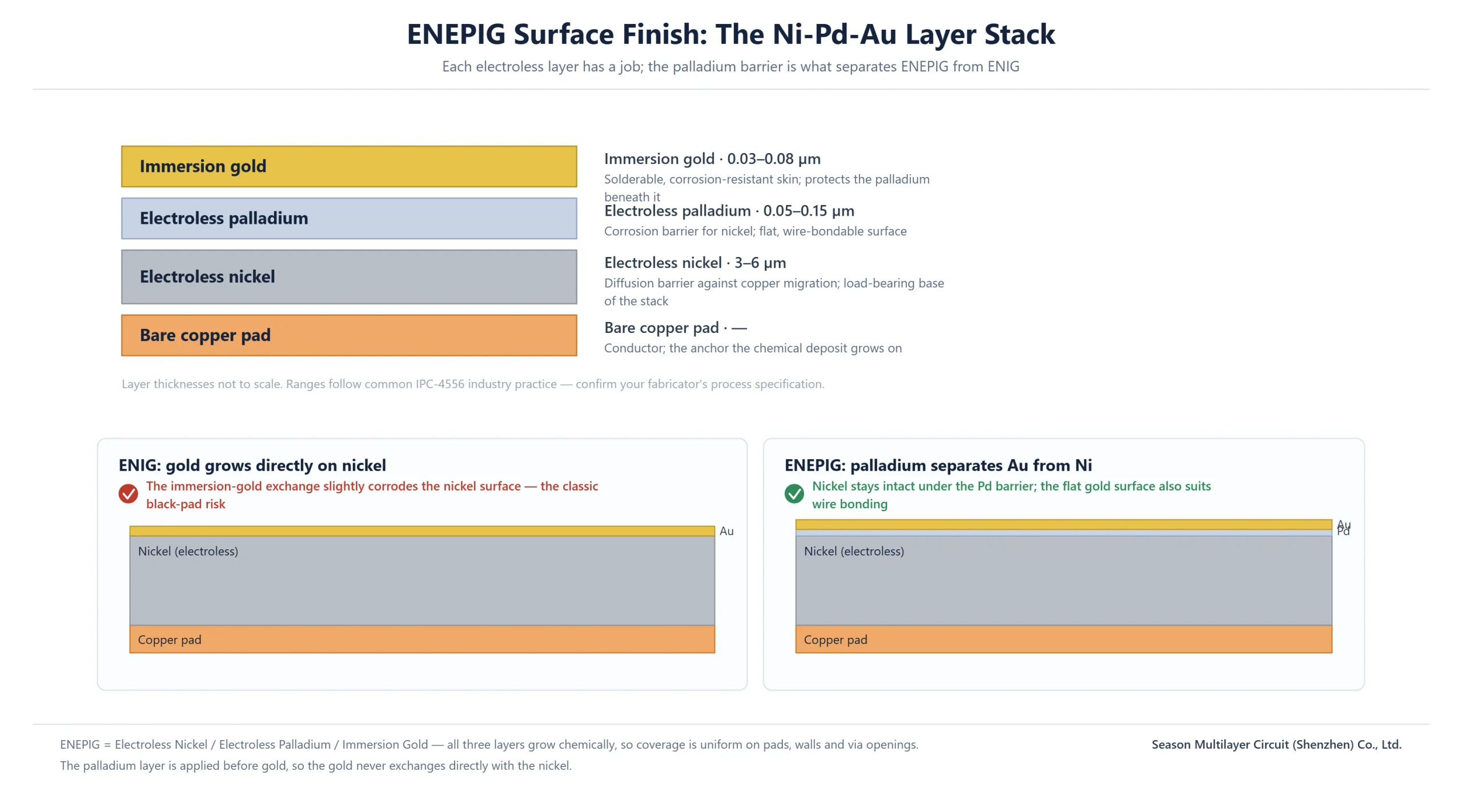
Treat the thickness values as typical industry practice rather than a universal recipe: the ranges align with the IPC-4556 convention, but individual fabricators tune them to their bath chemistry and end-market requirements. Always confirm the actual specification your fabricator will hold, and have it written on the travel documentation with the shipment.
ENIG vs ENEPIG: How the Palladium Layer Kills Black Pad
Black pad is an ENIG failure mode, not a plating cosmetic issue. In conventional ENIG, the immersion gold deposits by directly exchanging atoms with the nickel: gold ions from the bath take electrons from the nickel surface, and nickel dissolves in exchange. If the bath chemistry drifts, the exchange attacks the nickel along grain boundaries, leaving a corroded, brittle nickel–gold interface that looks fine until soldering — then BGA balls shear off along the weakened layer.
ENEPIG interrupts that reaction at the root. Palladium deposits on the nickel first, and the immersion gold then exchanges with the palladium instead of the nickel. The nickel surface never participates in the gold reaction, so hyper-corrosion of the nickel has nothing to latch onto. That single design change is why ENEPIG is the standard answer when a customer has been burned by black pad.
| Attribute | ENIG | ENEPIG |
|---|---|---|
| Deposit sequence | Nickel then immersion gold (direct exchange) | Nickel, palladium, then immersion gold (exchange with Pd) |
| Black pad risk | Inherent to the process; bath control dependent | Structurally avoided by the palladium barrier |
| Gold wire bonding | Not dependable; gold too thin over nickel | Reliable on the palladium/gold surface |
| Contact durability | Modest; soft thin gold wears through | Better; palladium adds wear resistance |
| Multiple lead-free reflows | Acceptable | Acceptable, with more margin |
| Relative cost | Baseline | Modest premium over ENIG |
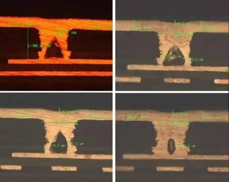
Black pad is not the only plating defect that shows up late. Microvia fill quality causes a separate family of assembly failures — see our guide to plating voids in microvias and how factories fix them for that side of the process.
Wire Bonding, Reflow and Assembly Behavior
The clearest technical differentiator is gold wire bonding. Thermosonic gold-ball bonding needs a surface that is hard enough to deform consistently, flat enough for the capillary, and noble enough to bond without a oxide-toughened interface. ENIG’s gold flash is too thin and sits directly on nickel, so ball bonds can lift. In ENEPIG the bond lands on the palladium layer — hard, uniform and self-supported — which is why module and chip-on-board assemblers moved to ENEPIG for wire-bonded pads.
For soldering, the gold skin is pore-free and stays oxide-free through normal shelf life, so wetting is fast and even across fine-pitch BGA and QFN lands. The finish also tolerates multiple lead-free reflow cycles without dewetting, which matters for double-sided assemblies and any board that passes through two or more thermal passes plus rework.
One caution belongs here: because gold dissolves into the solder joint, a properly controlled thin gold layer is an advantage, not a limitation. The palladium layer means the fabricator does not need to thicken the gold to protect the nickel — which keeps the deposit thin and the joint gold content low.
Contact Durability: Connectors, Edge Fingers and Insertion Cycles
Gold finishes on contacts fail by wear: the thin noble layer rubs through, exposed nickel oxidizes, and contact resistance climbs. Palladium raises the hardness of the surface the contact slides against, so ENEPIG holds contact resistance through noticeably more insertion cycles than ENIG on the same copper geometry. For board-to-board connectors, memory-module sockets and high-insertion interfaces specified without a separate hard-gold plating step, that margin is often the deciding factor.
Honest limits apply. Where a design specifies many hundreds of insertion cycles or carries RF current at the contact itself, electrolytic hard gold (with its thicker, nickel-underplated deposit) remains the stronger choice. ENEPIG is the durable, uniform, cost-balanced alternative — not a universal replacement for hard gold on every contact surface.
ENEPIG Cost Logic: Where the Money Actually Goes
Two cost facts shape the economics. First, gold is far more expensive per gram than palladium. Second, ENEPIG uses a very thin immersion gold layer — roughly a tenth of the thickness of a conventional electrolytic gold deposit — because the palladium layer, not the gold, does the protective work. Compared with full-area electrolytic gold, that typically makes ENEPIG the cheaper way to get a noble, wire-bondable surface across the whole panel.
Compared with ENIG, ENEPIG carries a real premium: one additional plating bath in the line plus the palladium metal itself. Expect quotes to sit modestly above ENIG for the same build, with the gap widening slightly as panel area consumed by pads increases. Because both palladium and gold trade on volatile metals markets, ask suppliers to itemize the finish as a line item and to state the quote’s validity window — that keeps offers comparable across fabricators.
The other economic lever is yield. The ENEPIG deposit cannot be locally reworked: a defective finish means scrapping the panel, which is painful on high-layer-count or controlled-impedance builds. A fabricator with strong bath controls and inline XRF thickness checks converts that risk into consistent first-pass yield — which is worth more than a small unit-price difference.
Process Control: What Your Fabricator Must Hold Steady
ENEPIG rewards discipline. The nickel, palladium and gold baths each have tight operating windows for temperature, pH and metal concentration, and the layers interact: contamination carried over from the nickel bath disturbs palladium nucleation, and a poor palladium surface degrades both the gold exchange and wire bonding. Ask prospective suppliers how they monitor bath impurities and how often they analyze and replenish each solution.
Thickness uniformity is the second watch item. Palladium in particular must land evenly — a coefficient of variation of 10% or better across the panel is a reasonable expectation to discuss — because thin spots become corrosion initiation points. Reputable lines verify thickness by X-ray fluorescence on production coupons and retain those readings with the job traveler.
Finally, ask about inspection and yield data rather than marketing claims: XRF logs, solderability test results on a sampling plan, and first-pass yield on comparable builds. A supplier running the finish daily for automotive or module customers will answer with numbers; one running it occasionally will answer with adjectives.
Where ENEPIG Fits: A Selection Table
The finish decision becomes easy when you match it to the dominant stress on the board: soldering only, wire bonding, mechanical contact, or cost. The table below condenses the guidance above into scenarios a project team actually faces.
| Application scenario | Good fit for ENEPIG? | Why |
|---|---|---|
| Automotive control units and long-life industrial boards | Yes | Corrosion barrier and reflow tolerance support long field life in harsh environments |
| Gold wire bonding / chip-on-board modules | Yes — preferred | Wire bonds land on the hard, flat palladium surface instead of thin gold on nickel |
| High-insertion connectors and sockets | Yes | Palladium hardening resists wear-through across repeated mating cycles |
| Fine-pitch BGA and QFN soldering | Yes | Uniform, pore-free gold skin gives fast, even wetting |
| Millimeter-wave and sensitive RF pads | Conditional | Where contact-level conductivity dominates, electrolytic gold can still win — review case by case |
| Cost-driven high-volume consumer boards | Usually no | ENIG or OSP meet the requirement at a lower finish cost |
To see the finish in context of the whole build, pair this with our PCB materials and laminates guide when the substrate choice is also open, and with our automotive PCB manufacturing capability page for the reliability context behind the first row.
How to Specify an ENEPIG Surface Finish on Your Fab Drawing
A vague finish callout is the fastest way to get non-comparable quotes. Specify the ENEPIG surface finish with the same precision you expect back in the certificate of conformance, and the fabrication notes do the negotiating for you. Put these items in the drawing notes:
- Finish name spelled out — Electroless Nickel / Electroless Palladium / Immersion Gold (ENEPIG) — with the applicable IPC-4556 specification referenced.
- Thickness callouts per layer: nickel 3–6 µm, palladium 0.05–0.15 µm, gold 0.03–0.08 µm, unless your end market dictates otherwise.
- Verification method: XRF thickness measurement on coupon per lot, with results retained and available on request.
- Solderability requirement: wetting balance or dip-and-look testing per the applicable IPC solderability method, on a stated sampling plan.
- Gold wire bonding callout where applicable — mark the pads that must accept gold wire bonds so the fabricator holds palladium thickness on them.
With a complete callout, quotes from different fabricators describe the same product — which makes relative price comparisons meaningful instead of apples-to-oranges. For context on how the finish fits into the total quote, our article on what drives 4-layer PCB cost breaks the quote structure down line by line.
ENEPIG Surface Finish: Key Takeaways
For teams weighing the finish on a current project, these are the points that should drive the decision:
- The palladium barrier is the whole story: it removes the black-pad mechanism structurally rather than by bath discipline.
- Wire bonding on ENEPIG is dependable where ENIG is not — make the callout explicit on wire-bonded pads.
- Relative cost sits modestly above ENIG and usually below full-area electrolytic gold, driven by thin gold over palladium.
- The finish cannot be reworked locally, so supplier process control and yield data matter more than unit price.
- Specify layer thicknesses, XRF verification and solderability testing on the drawing so all quotes describe the same board.
If a current build has an unexplained assembly failure and ENIG is in the stack, an interface cross-section is usually enough to confirm or rule out black pad before you change finishes — and it costs far less than guessing.
Frequently Asked Questions
What is the ENEPIG surface finish?
ENEPIG stands for Electroless Nickel, Electroless Palladium, Immersion Gold. Three layers grow chemically on every exposed copper feature: nickel for the diffusion barrier and mechanical base, palladium as a corrosion barrier and wire-bondable surface, and a thin immersion gold flash for solderability and tarnish protection. All three deposit without electric current, so coverage stays uniform on fine-pitch pads and inside via openings.
How is ENEPIG different from ENIG?
The difference is the palladium layer. In ENIG, immersion gold deposits by exchanging directly with nickel, which can hyper-corrode the nickel interface and produce black pad. In ENEPIG, palladium deposits on the nickel first and the gold exchanges with the palladium instead, so the nickel never participates. ENEPIG also supports gold wire bonding and resists contact wear better than ENIG.
Does ENEPIG support gold wire bonding?
Yes, reliably. The wire bond lands on the electroless palladium layer, which is hard, flat and uniform — the conditions thermosonic gold-ball bonding needs. On ENIG, bonds land on a very thin gold layer directly over nickel and can lift. If your design mixes wire-bonded pads with soldered areas, mark the wire-bond pads on the drawing so palladium thickness is held there.
Why does ENEPIG cost more than ENIG?
Two reasons: one additional plating bath in the line (palladium) and the palladium metal itself, which adds to the precious-metal content of the deposit. The premium over ENIG is modest, and ENEPIG usually undercuts full-area electrolytic gold because its immersion gold layer is about a tenth of the thickness. Precious-metal market volatility affects both finishes, so ask for an itemized finish line and a quote validity window.
Can a defective ENEPIG finish be reworked?
Not locally. The plated layers cannot be stripped and re-deposited on selected pads the way some defects can be touched up elsewhere in fabrication, so a defective finish generally means scrapping the panel. That makes the fabricator’s bath control, XRF thickness monitoring and first-pass yield on comparable builds the most important quality signals to check before placing an order.
Which ENEPIG plating thicknesses should I put on my drawing?
Common industry practice, aligned with the IPC-4556 convention, is nickel 3–6 µm, palladium 0.05–0.15 µm and immersion gold 0.03–0.08 µm. Confirm the exact values with your fabricator against their process specification and your end market, and require XRF verification per lot with the readings retained on the job traveler.
Is ENEPIG suitable for lead-free assembly and multiple reflows?
Yes. The pore-free gold skin stays oxide-free through normal shelf life and wets quickly with lead-free solders, and the finish tolerates several reflow cycles without dewetting — relevant for double-sided assemblies and boards passing through multiple thermal processes. The thin gold layer also keeps dissolved gold content in the solder joint low.
Get Your Surface Finish Reviewed Before You Order
Submitting Gerber data and a stackup sketch is enough for a meaningful engineering review of your finish choice — including an honest check of whether ENEPIG, ENIG or selective hard gold is the right call for your pads. Our PCB manufacturing services page explains what to include so the review comes back with real numbers instead of a brochure.