Book Appointment Now

E1.S SSD PCB design explained: EDSFF thickness classes, layer counts, PCIe 5.0 impedance rules and the fabrication limits that decide yield on narrow carriers.
E1.S SSD PCB Design: EDSFF Carrier Board Stackup and Fabrication Rules
Data center drives are moving off the 2.5-inch footprint, and the E1.S SSD is the form factor replacing it in density-critical 1U servers. What buyers usually underestimate is that the drive lives or dies on its carrier board: a narrow PCB that must escape four PCIe lanes, feed a 25 W controller and NAND array, and survive hot-plug service – all inside a 31.5 mm wide envelope. This guide walks through the E1.S SSD PCB decisions that matter: thickness classes, stackup, impedance, materials and the fabrication rules that decide yield.
The numbers here follow the public EDSFF specifications (the SFF-TA-1006 family) and the capability set of our factory – 2 to 30 layers, 0.1 mm laser microvias and 2/2 mil line and space as standard. Where a value depends on your design, we flag it as a decision to confirm at engineering review rather than quote a blanket figure.
Table of Contents
- What an E1.S SSD Carrier Board Actually Is
- E1.S SSD PCB Dimensions: Five Thickness Classes, One Width Logic
- E1.S SSD PCB Stackup: Layer Count Follows the Interface
- Escaping the Connector in a 31.5 mm Wide Board
- Impedance Control and Insertion Loss for PCIe 4.0 and 5.0
- Material Selection for Gen4 and Gen5 E1.S SSD PCB Builds
- Power Delivery, PLP Capacitors and Thermal Coupling
- Fabrication Rules That Decide Yield on Narrow Carriers
- A DFM Checklist Before You Release E1.S Carrier Gerbers
- FAQ
- Get Your E1.S SSD PCB Stackup Reviewed Before Layout Freeze
What an E1.S SSD Carrier Board Actually Is
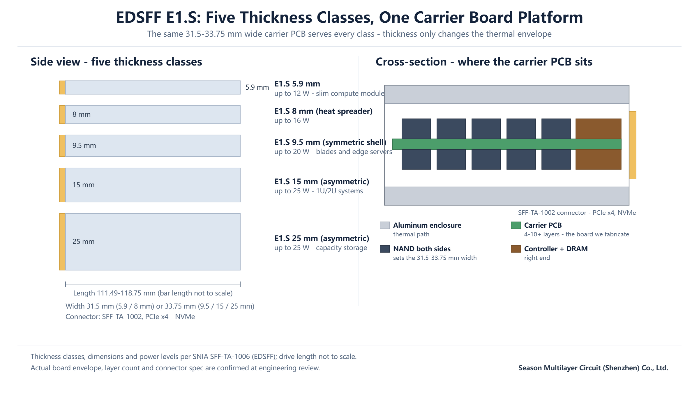
E1.S is the short member of the EDSFF (Enterprise and Data Center SSD Form Factor) family, standardised by SNIA in the SFF-TA-1006 series. A finished drive measures 31.5 mm or 33.75 mm wide and 111.49 mm or 118.75 mm long, in five thickness classes from 5.9 mm to 25 mm. Drives mount vertically in front-serviceable bays, which is how a 1U chassis reaches 32 drives without a single expansion slot.
Inside the aluminum shell there is no mystery: a carrier PCB carries the controller, DRAM and NAND packages on both faces, plus power-loss protection capacitors where the product requires them. The SFF-TA-1002 connector at the drive’s edge carries four PCIe lanes, with NVMe as the block protocol. Everything else – fins, heat spreaders, latches – is sheet metal whose shape follows the thickness class.
For a purchasing team, that reframes the supplier question. You are not buying “an SSD form factor”; you are buying a narrow, high-layer-count, impedance-controlled PCB whose mechanical envelope is fixed by a public standard. The sooner the carrier board is designed against that envelope, the fewer respins the project needs.
E1.S SSD PCB Dimensions: Five Thickness Classes, One Width Logic
The five thickness classes exist because thermal headroom, not connector logic, sets what a drive can do. The two slim classes target low-power compute modules, the symmetric 9.5 mm class serves blades and edge servers, and the asymmetric 15 mm and 25 mm classes absorb the 25 W envelopes of performance and capacity arrays. The class you pick cascades directly into the E1.S SSD PCB: it fixes board width, allowed component heights and how much copper the power tree can afford.
| Thickness class | Max power | Board width | Typical systems |
|---|---|---|---|
| 5.9 mm | 12 W | 31.5 mm | Slim compute modules |
| 8 mm (heat spreader) | 16 W | 31.5 mm | Low-profile compute |
| 9.5 mm (symmetric shell) | 20 W | 33.75 mm | Blade and edge servers |
| 15 mm (asymmetric shell) | 25 W | 33.75 mm | 1U/2U performance storage |
| 25 mm (asymmetric shell) | 25 W | 33.75 mm | High-capacity storage arrays |
Board outline follows the class. The 5.9 mm and 8 mm variants carry a 31.5 mm wide board; the three enclosed classes widen to 33.75 mm to open room for a second row of NAND. Length differs by 7 mm between the bare 111.49 mm boards and the 118.75 mm enclosed formats – enough to matter when you plan connector keep-outs and sensor placement. Because the drive mates through gold-plated edge fingers rather than a separate plug, the fabrication spec must call out hard-gold edge plating on the card edge, not just a standard surface finish.
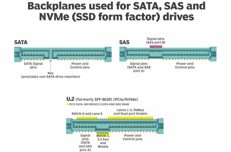
If your platform standardised on 2.5-inch bays instead of EDSFF, the same decisions reappear in a bigger envelope – our U.2 SSD PCB design guide covers the SFF-8639 side of the comparison.
E1.S SSD PCB Stackup: Layer Count Follows the Interface
Layer count on an E1.S SSD PCB is a routing problem before it is a cost problem. Four PCIe lanes leave the edge connector as differential pairs that must reach the controller within a few millimetres of escaped trace, and a modern controller fans out to eight or more NAND channels across both faces of the board. Our shipped storage boards show the pattern: a 4-layer SATA SSD PCB carries a bottleneck-free SATA link, while 10-layer builds are the norm for M.2 NVMe designs at PCIe 4.0 speeds.
| Interface class | Typical carrier layers | What drives the count |
|---|---|---|
| SATA 6 Gb/s | 4-6 | One differential pair, power tree, NAND on two faces |
| PCIe 4.0 x4 NVMe | 6-10 | Four lane pairs plus clock, eight NAND channels, PLP bank |
| PCIe 5.0 x4 NVMe or dual-port | 10+ | Escape density, reference planes, power integrity |
Keep the stackup symmetric about the centreline even where a cheaper asymmetric build would pass design-rule checks. A thin board sandwiched between NAND on both faces warps during reflow if copper and dielectric distribution is unbalanced, and warp is what you discover at second-side assembly, when the edge fingers no longer seat cleanly into the backplane.
Escaping the Connector in a 31.5 mm Wide Board
The E1.S envelope leaves roughly 25 mm of usable routing width between the connector edge and the controller land field. Four lanes, a reference clock pair and the sideband group all leave that region in the first 10 to 15 mm, which is why breakout density – not channel length – is usually the binding constraint on this board.
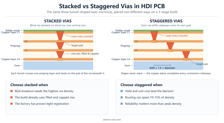
The practical toolkit is the same one HDI boards use. Laser microvias at 0.1 mm reach the controller’s fine-pitch lands through the escape channels; via-in-pad with resin fill and capping reclaims pin fields a conventional fan-out would consume; and 2/2 mil line and space (1.8/1.8 mil on sample builds) keeps pairs routable between adjacent lands. IPC-2226 collects the microvia design rules most data center hardware teams cite in their own design guides.
Impedance Control and Insertion Loss for PCIe 4.0 and 5.0
PCIe routing on a carrier board targets 85 Ω differential impedance. A capable fabricator holds ±10% as standard and ±8% or ±5% when the design asks for it – the tighter numbers cost more and are only worth specifying when your loss budget is genuinely marginal. Put the controlled-impedance callout, per pair class, on the fabrication drawing, and ask for TDR coupons from every production panel.
Insertion loss is the quieter problem. At PCIe 5.0 the 32 GT/s signalling puts the Nyquist frequency at 16 GHz, and the entire channel – host board, connector, carrier, drive-side traces – shares one loss budget measured in a few tens of dB. The carrier’s contribution is set by laminate choice and via stubs; on a board this thin, stubs are short, so material selection and return-path discipline dominate the result.
Material Selection for Gen4 and Gen5 E1.S SSD PCB Builds
For Gen4 carriers, a mid-Tg FR-4 with a modest dissipation factor is usually sufficient, and it keeps the laminate commodity. Gen5 carriers reward a dedicated low-loss laminate chosen for dissipation factor first and price second. As planning numbers: moving from standard FR-4 to a low-loss system adds roughly 20-60% to bare-board cost at the same layer count, and moving up one HDI stage typically adds 30-100% to board cost. Our PCB laminate selection guide walks the full trade space.
Halogen-free is no longer a special request: a Tg ≥150 halogen-free grade such as S1150G slots into carrier builds where the end customer’s environmental specification demands it. For thermal management, note that the aluminum enclosure – not the PCB – is the primary heat path in E1.S. That is one reason heavy-copper carrier boards are rare here; put copper where the power tree needs it and let the shell do the rest.
Power Delivery, PLP Capacitors and Thermal Coupling
Power arrives on the connector as a 12 V rail and is converted locally to the controller, NAND and DRAM rails. The space hogs are the power-loss protection capacitors: enterprise carriers stack ceramic banks along the board’s long edge, and the bank height often decides whether the design fits a 9.5 mm class or needs 15 mm. Place the PLP bank and the buck converters before you commit the NAND floorplan.
Thermally, the PCB’s job is to spread heat from controller and NAND into the shell’s thermal interface, not to sink it. Continuous copper planes under the controller, stitched toward the shell interface with thermal vias, do more for a 25 W class drive than an exotic laminate does. The 12 W to 25 W spread across thickness classes is exactly why the stackup conversation belongs in the same meeting as the mechanical one.
Fabrication Rules That Decide Yield on Narrow Carriers
Narrow carriers panelize efficiently – a production panel carries many E1.S blanks – so panel utilisation is a cost lever worth discussing with the fabricator before the outline is final. Rails, fiducials and the impedance coupons should be planned with the panel in mind, not added after layout. The same is true for any portable SSD PCB built in volume: outline decisions made in CAD echo through yield for the life of the product.
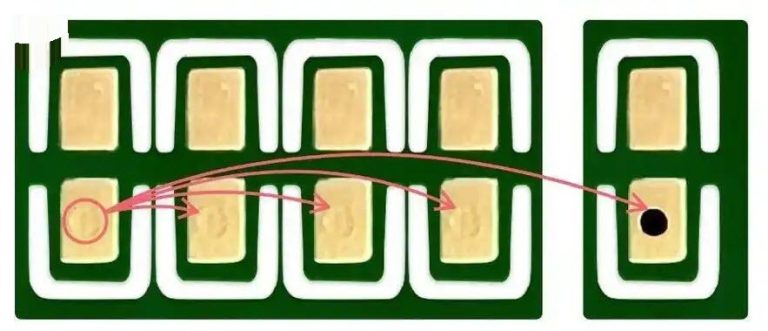
Two process notes save respins. First, the edge fingers need hard gold over nickel with a defined thickness; a standard ENIG line is not an edge-plating process, and OSP cannot protect fingers at all. Second, wherever a via sits under the controller or inside a NAND pad, specify filled and capped vias explicitly – the copper filled via process is what keeps pads flat for second-side assembly and blocks solder wicking into the barrel.
A DFM Checklist Before You Release E1.S Carrier Gerbers
Before the data package leaves your team, run it against this list – it covers the items our engineering review flags most often on EDSFF-class carriers:
- Stackup drawing with dielectric heights, copper weights and the impedance target for every pair class
- Edge-finger plating spec: hard gold over nickel, thickness and tip length
- Material callout with permitted substitutes named, so quotes stay comparable
- Via schedule: which vias are filled, capped or tented – per via class, not one blanket note
- Copper balance across layers for reflow warp control
- Panel and rail intent, so coupons and fiducials land where the fabricator needs them
- Acceptance class – IPC-6012 Class 3 is the norm for enterprise carriers
- Controlled-impedance coupon plan and test frequency
A reviewer who can read the Gerber data against this list will catch most respin drivers in a single pass.
Frequently Asked Questions
What is an E1.S SSD?
It is a short, vertical, hot-pluggable enterprise SSD defined by the EDSFF standards (SFF-TA-1006 family). It speaks NVMe over four PCIe lanes, mounts in front-serviceable 1U bays, and comes in thickness classes from 5.9 mm to 25 mm so thermal capability scales with the chassis design.
How big is an E1.S SSD PCB?
The board inside is 31.5 mm wide on the slim 5.9 mm and 8 mm classes and 33.75 mm wide on the 9.5 mm, 15 mm and 25 mm classes. Length is 111.49 mm or 118.75 mm depending on the enclosure format. Thickness of the drive shell – not the PCB – is what varies across the five classes.
Is E1.S better than M.2 for servers?
For data center use, generally yes: E1.S provides a standardised thermal envelope of up to 25 W against the much tighter M.2 budget, native hot-plug serviceability, and a shell designed for vertical airflow. M.2 remains the right choice for client devices where a socket on the motherboard beats a drive bay.
How many layers does an E1.S carrier PCB need?
Plan on 4-6 layers for SATA-class links, 6-10 for PCIe 4.0 x4 NVMe, and 10 or more for PCIe 5.0 or dual-port designs. The right answer depends on NAND channel count and escape density, so treat the layer count as a routing calculation confirmed at engineering review, not a fixed rule.
What impedance do PCIe traces on an E1.S SSD PCB use?
PCIe differential pairs are designed for 85 Ω. Fabricators hold ±10% as a standard tolerance and can commit to ±8% or ±5% where the design needs it. Specify the target per pair class on the fabrication drawing and verify with TDR coupons from each production panel.
Can standard FR-4 be used for a Gen5 E1.S carrier?
Usually not with confidence. PCIe 5.0’s 16 GHz Nyquist content makes dissipation factor the dominant loss term, and a low-loss laminate is the safer call. Gen3 and Gen4 carriers routinely ship on mid-Tg FR-4 with acceptable margins. If your channel is short and the backplane is forgiving, ask for a loss simulation before paying the laminate premium.
Who manufactures E1.S SSD carrier boards?
Specialist PCB fabricators with fine-line and HDI capability. Our factory builds storage carriers from 4-layer SATA boards to 10-layer NVMe designs, with 0.1 mm laser microvias, 2/2 mil line and space, and hard-gold edge fingers as standard processes. Send the stackup intent for a buildability review before layout freeze.
Get Your E1.S SSD PCB Stackup Reviewed Before Layout Freeze
Send your stackup intent, connector finger spec and NAND floorplan, and our engineering team will review layer count, escape density and impedance targets against the E1.S envelope – then quote the build. Start on the PCB manufacturing services page, or browse our shipped 10-layer M.2 SSD PCB as a reference build.