Book Appointment Now

PCB prototyping builds a small batch of boards on a short turnaround to validate a design before mass production. See the process, applications and capabilities.
What Is PCB Prototyping? A Complete Guide to Rapid PCB Prototype Manufacturing
I. What Is PCB Prototyping?
Definition of PCB Prototyping and Rapid Prototyping
PCB prototyping (also called PCB rapid prototyping or PCB fast sample) is the process of manufacturing a small number of printed circuit boards in a short turnaround time—typically 24 to 96 hours—to validate a design before committing to full-scale production. These prototype boards are electrically and mechanically identical to the final production PCBs, allowing engineers to test form factor, signal integrity, thermal performance, and manufacturing feasibility without waiting weeks for a standard production run.
At 998PCB Group / Season Multilayer Circuit, PCB prototyping is a core service. Established in 2006, our Shenzhen facility handles everything from simple 2-layer boards to complex HDI PCBs with up to 14 layers, all available on expedited 48/72/96-hour schedules.
Why PCB Prototyping Matters in Electronics Development
In modern electronics development, time-to-market is often the single most critical competitive factor. A delay of two weeks at the PCB stage can cascade into months of delay at the product level. Rapid prototyping addresses this by compressing the manufacturing cycle from the standard 10–15 business days down to as little as 24 hours for single-layer and double-layer boards, and 48–96 hours for multilayer and HDI designs.
Beyond speed, prototyping serves several vital purposes: it validates the electrical design (signal integrity, power distribution, impedance control), confirms manufacturability (DFM compliance, minimum annular ring, trace width/spacing), and provides a physical sample for mechanical fit-check (enclosure clearance, connector alignment, mounting hole positions). Without a prototype, these issues would only surface during mass production—when fixing them costs 100x more.
Rapid PCB Prototyping vs. Standard PCB Manufacturing
The key difference between PCB prototyping and standard PCB manufacturing is not quality—it is scheduling and process flow. Standard manufacturing batches panels together to optimize material usage and press cycle efficiency. Rapid prototyping prioritizes a single panel or a few panels through the production line, bypassing batch scheduling. This means some process steps (like lamination) may use smaller press plates, and certain parallel processes (like drilling and plating) are done sequentially rather than simultaneously.
The trade-off is cost: a 96-hour prototype typically costs 1.5–3x more per board than a standard production board of the same design. However, for most product development teams, the weeks saved in time-to-market far outweigh the additional per-board cost. A reputable PCB manufacturer will offer both options and help you choose based on your project timeline and budget.
II. The PCB Prototyping Process: Step by Step
The PCB prototyping process follows the same fundamental manufacturing steps as standard PCB production, but with optimized scheduling and prioritized workflow. Below, we walk through each stage as it is practiced at 998PCB Group / Season Multilayer Circuit for our Shenzhen rapid prototyping service.
Step 1: PCB Prototyping Design Phase
PCB design is the starting point of the entire PCB prototyping process. Layout engineers use professional EDA software such as Altium Designer, KiCad, Eagle, or PADS to create the circuit schematic and PCB layout. During this phase, designers must pay close attention to component placement, trace routing, signal integrity, power integrity, and thermal management.
For prototype designs, it is especially important to follow Design for Manufacturing (DFM) guidelines provided by the PCB manufacturer. Common DFM considerations include minimum trace width, minimum annular ring, drill-to-copper clearance, and panel utilization. Submitting a DFM-compliant design reduces the risk of manufacturing delays or board rejects. At 998PCB Group, our engineering team provides free DFM review for all prototype orders.
Step 2: PCB Prototyping Material Selection
The choice of PCB substrate material directly affects the board’s electrical performance, thermal characteristics, and cost. The most common materials include:
- FR-4 (Standard Tg ≥140°C) — the workhorse for most consumer electronics, IoT devices, and industrial controls.
- High-Tg FR-4 (Tg ≥170°C) — for applications requiring better thermal stability and lead-free soldering compatibility.
- High-Frequency Laminates (Rogers RO4350B/RO4003C, Panasonic Megtron 6) — for RF and microwave circuits requiring low dielectric loss.
- Aluminum / Metal Core PCB (MCPCB) — for high-power LED lighting and power electronics requiring superior heat dissipation.
- Polyimide — for flexible and rigid-flex circuits used in wearable devices and compact consumer electronics.
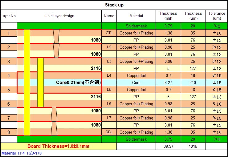
For multilayer and HDI prototypes, the stackup design also determines the dielectric thickness, copper weight, and impedance control layers. The image below shows a typical 8-layer 2-stage HDI lamination structure with three lamination cycles and two laser-drilling steps.
Step 3: PCB Prototyping File Generation (Gerber Files)
Once the PCB layout is finalized, the designer generates a set of Gerber files (or ODB++ / IPC-2581 format) that contain all the information needed by the PCB manufacturer. A complete file set includes copper layers, solder mask layers, silkscreen layers, drill files (plated and non-plated), and board outline. The manufacturer also requires a bill of materials (BOM) and pick-and-place file if PCBA (assembly) service is needed.
For rapid prototyping, we recommend submitting files in RS-274X Gerber format (not older RS-274D), as it embeds aperture definitions and requires less back-and-forth clarification. At 998PCB Group, our online DFM check tool automatically verifies your files for common issues before production begins.
Step 4: PCB Prototyping Fabrication
In PCB prototyping, the fabrication stage transforms raw laminate panels into functional circuit boards through a series of chemical and mechanical processes. For a standard multilayer PCB, the key steps include inner layer imaging and etching, oxide treatment and layup, lamination press, drilling (mechanical for through-holes, laser for micro-vias in HDI), desmear and copper plating, outer layer imaging and etching, solder mask application, and surface finish (HASL, ENIG, OSP, or immersion silver/tin).
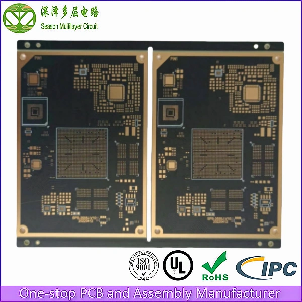
For HDI prototypes, additional steps include laser drilling of blind/buried vias, sequential lamination cycles, and plasma desmear. The 10-layer 1-stage HDI sample shown below illustrates a typical expedited HDI prototype—from raw core to finished board—manufactured on our 96-hour schedule. For a full walkthrough of how multilayer and HDI boards are fabricated layer by layer, see our 8-layer 2-stage HDI PCB manufacturing process guide.
Step 5: PCB Prototyping Quality Inspection and AOI
After fabrication, every prototype board undergoes a rigorous quality inspection process. This includes Automated Optical Inspection (AOI) to detect trace opens/shorts, pad defects, and solder mask issues; flying probe testing or fixture-based ICT to verify electrical continuity and isolation; and visual inspection under magnification for surface defects, via fill quality, and finish uniformity.
For HDI and high-layer-count prototypes, we also perform cross-section analysis on sample boards to verify via copper thickness, lalignment registration, and dielectric thickness. Only boards that pass all inspection criteria are released to the customer. This inspection-first philosophy is why 998PCB Group maintains a defect rate below 200 PPM (parts per million) even on expedited orders.
Step 6: PCB Prototyping Functional Testing
Functional testing is the stage where the prototype PCB is powered up and tested under real-world conditions. Test engineers use oscilloscopes, logic analyzers, signal generators, and multimeters to verify that the circuit performs according to the design specification. Key measurements include signal integrity (eye diagrams, jitter, rise/fall time), power rail voltage and ripple, clock frequency and phase, and thermal behavior under load.
Any anomalies detected during functional testing feed directly back to the design team for analysis and correction. This design–build–test–iterate loop is the core value proposition of rapid prototyping: it allows teams to catch and fix issues early, when the cost of change is minimal, rather than during mass production when tooling and inventory commitments make changes expensive.
Step 7: PCB Prototyping Evaluation and Design Iteration
Based on functional testing results, the design team evaluates the prototype’s performance against requirements and decides whether the design is ready for production or requires another iteration. Common iteration triggers include impedance mismatches, EMI/EMC failures, thermal hotspots, mechanical fit issues, or manufacturability concerns identified by the PCB fabricator.
Each iteration typically takes 3–7 days depending on complexity, and most products require 2–3 prototype cycles before reaching production-ready status. By using rapid prototyping services, teams can compress the total design cycle from months to weeks, achieving faster time-to-market and higher product quality.
III. Applications of PCB Prototyping
Prototype manufacturing plays a vital role across the entire electronics industry. From startup innovation to enterprise R&D, rapid access to physical circuit boards accelerates development and de-risks product launches. Below we explore the five most common applications.
Prototype Development and Design Validation
In new product development, the first physical prototype is a critical milestone. PCB prototyping allows design teams to move from CAD model to real hardware in days, not weeks. Engineers can physically test form factor, connector mating, thermal performance, and signal integrity—things that simulations cannot fully predict. Early prototypes also enable regulatory pre-compliance testing (FCC, CE, IC) to identify potential certification risks before the final design is locked in.
Production Line Testing and Process Validation
Before committing to volume production, manufacturing teams need to validate the production line itself. Prototype boards are used to qualify test fixtures, verify solder paste stencil aperture designs, optimize reflow oven profiles, and validate automated inspection programs. Running a small batch of prototype boards through the full PCBA process line helps identify process issues early, reducing the risk of yield loss and rework when full production begins.
Education and Training
In universities and technical training centers, PCB prototyping is an essential teaching tool. Students learn PCB design principles, manufacturing processes, and testing methodologies by working with real boards. The short turnaround of rapid prototyping services means students can complete a full design–build–test cycle within a single semester or even a single lab module. This hands-on experience bridges the gap between theoretical knowledge and real-world engineering practice.
Small-Batch Production
For low-volume or custom products, PCB prototyping offers a flexible alternative to volume production. Products such as industrial control modules, medical device sub-assemblies, aerospace test equipment, and research instruments often require 10–100 boards—too few for full production tooling, but too many for hand soldering. Rapid prototyping fills this gap with cost-effective small-batch runs on 48–96 hour schedules, with the same quality standards as volume production.
Startup Innovation Projects
For startups and entrepreneurs, PCB prototyping is a strategic enabler. A working hardware prototype is often the key asset needed to secure investor funding, demonstrate product-market fit, and prepare for crowdfunding campaigns. The ability to iterate quickly on hardware design—testing new features, fixing bugs, and refining the user experience—is what separates successful hardware startups from those that stall in development. At 998PCB Group, we support qualifying startups with free prototyping services to help them bring their innovations to market faster.
IV. PCB Prototyping Turnaround Times and Capabilities
Standard Turnaround (5–10 Business Days)
Standard PCB manufacturing typically takes 5–10 business days for 2–6 layer boards, and 10–15 days for high-layer-count or HDI designs. This timeline allows the manufacturer to batch panels for optimal material utilization, schedule press cycles efficiently, and perform all quality inspection steps in parallel. Standard turnaround is the most cost-effective option when the project schedule allows it.
Expedited Turnaround (24/48/72/96 Hours)
For urgent projects, 998PCB Group offers four tiers of expedited quick-turn prototyping:
- 24-Hour — single and double-layer boards up to 4 layers (standard FR-4)
- 48-Hour — 4–6 layer boards with standard vias and surface finish
- 72-Hour — 6–10 layer boards, including HDI 1-stage designs
- 96-Hour — up to 14-layer boards, HDI 2-stage, high-frequency materials, and special surface finishes (ENIG, Immersion Silver)
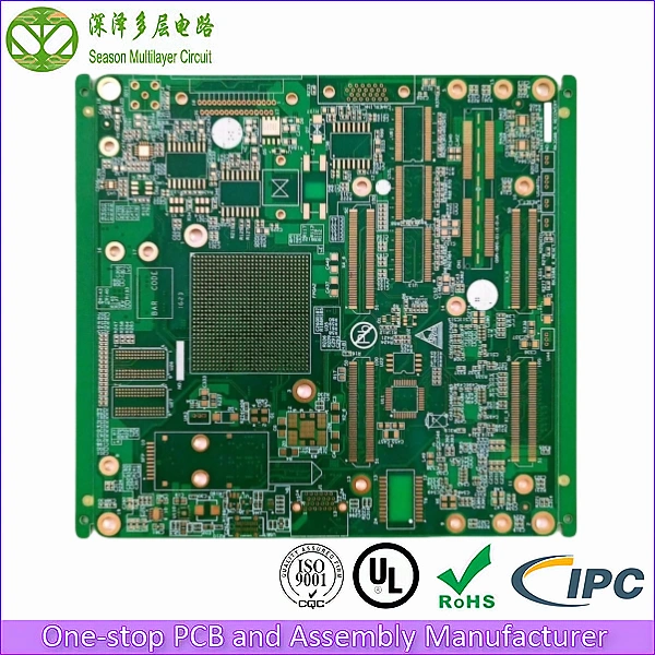
The 14-layer board shown below was manufactured on our 96-hour expedited schedule, demonstrating that complex multilayer designs can be prototyped quickly when the production line is configured for rapid turnaround.
Not all designs are eligible for the fastest turnaround tiers. Factors that may require a longer schedule include blind/buried via stacks, sequential lamination cycles, impedance-controlled traces requiring TDR testing, hard gold fingers, and non-standard laminate materials. Our engineering team reviews each expedited order to confirm feasibility before accepting the schedule commitment.
Key Takeaways on PCB Prototyping
- PCB prototyping compresses the manufacturing cycle from weeks to hours, enabling faster design–build–test iteration.
- The process includes seven core steps: design, material selection, file generation, fabrication, inspection, functional testing, and evaluation.
- Rapid prototyping costs 1.5–3x more per board than standard production, but the time saved typically justifies the premium for development projects.
- Applications span the entire electronics industry: from startups to enterprise R&D, from education to small-batch production.
- 998PCB Group / Season Multilayer Circuit offers 24/48/72/96-hour expedited prototyping for up to 14-layer HDI boards from our Shenzhen facility.
- DFM-compliant design and complete Gerber file sets are essential for avoiding delays in the expedited manufacturing workflow.
Whether you are validating a new design, qualifying a production line, or building investor demo hardware, PCB prototyping is the bridge between concept and reality.
Conclusion: PCB Prototyping at This Factory
PCB prototyping is not just a manufacturing service—it is a strategic capability that determines how quickly your product moves from idea to market. By understanding the seven-step prototyping process, choosing the right materials, and working with an experienced manufacturing partner, you can compress your development timeline by weeks or even months.
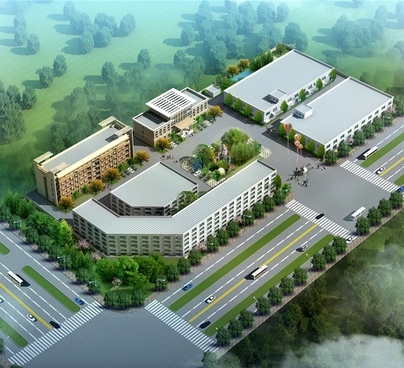
Since 2006, 998PCB Group / Season Multilayer Circuit has provided rapid PCB prototyping services from our Shenzhen manufacturing facility. We handle everything from simple 2-layer boards to complex 14-layer HDI designs, with expedited schedules as fast as 24 hours. Our in-house engineering team provides free DFM review for every order, ensuring your design is optimized for manufacturability before production begins.
Ready to start your PCB prototype? Contact us today for a free quote, or learn more about our PCB manufacturing services. For our Chinese-language resources on PCB prototyping, visit our 998pcb.com blog.
Frequently Asked Questions About PCB Prototyping
How fast can a PCB prototype be manufactured?
Standard prototypes take 5-10 business days. Expedited tiers run 24/48/72/96 hours: 24-hour service covers single and double-layer boards up to 4 layers, 48-hour covers 4-6 layer boards, 72-hour covers 6-10 layer boards including HDI 1-stage designs, and 96-hour covers up to 14-layer boards with HDI 2-stage structures or special surface finishes. Complex features such as blind/buried via stacks or impedance control may require a longer schedule.
What does PCB quick turn mean?
PCB quick turn refers to prototype fabrication on a compressed schedule, typically 24 to 96 hours, where your order is prioritized on the production line. The manufacturing process itself is identical to standard fabrication; the difference is scheduling priority, which is why quick turn service carries a premium and not every design qualifies for the fastest tiers.
How much more does a PCB prototype cost than mass production?
A prototype board typically costs 1.5-3x more per board than the same design in volume production, because setup, tooling, and engineering review are amortized over a small quantity. For most development teams the weeks saved in time to market outweigh the per-board premium, and issues caught at the prototype stage prevent far more expensive field failures.
Do you offer PCB prototype assembly services?
Yes. Beyond bare board fabrication, 998PCB Group provides prototype assembly (PCBA) including SMT placement, through-hole soldering, AOI inspection, and functional testing, so you can receive fully populated and tested prototype boards from the same order.
How many prototype iterations should I plan before mass production?
Most hardware teams plan two to three iterations: the first validates connectivity and power delivery, the second refines layout and thermal performance, and a final pilot run confirms the design is ready for low volume or mass production. Building one or two spare panels into each prototype order keeps the schedule flexible if a respin is needed.
What files do I need to start a PCB prototype?
RS-274X Gerber files with drill data are the minimum for fabrication. Include a pick-and-place file and BOM if you need assembly, plus impedance and stackup requirements for controlled-impedance designs. Our free DFM review checks your files for common manufacturability issues before production begins.
For a quick cost baseline on a 6–20 layer design, the instant PCB quote tool prices the board from its headline parameters in seconds, before any file is sent.