Book Appointment Now

How an 8-layer 2-stage HDI PCB is built: two lamination cycles with laser microvias, from inner-layer imaging through plating, solder mask and final test.
8-Layer 2-Stage HDI PCB Manufacturing Process: Complete Step-by-Step Guide
I. Overview of the 8-Layer 2-Stage HDI PCB Manufacturing Process
What is an 8-Layer 2-Stage HDI PCB?
The 8-layer 2-stage HDI PCB manufacturing process produces a high-density interconnect printed circuit board built using two sequential lamination cycles with laser-drilled microvias between each stage. It is the most widely used stackup for smartphones, tablets, IoT devices, and 5G modules where fine-pitch BGAs (0.4mm and below) must be routed without sacrificing signal integrity. In a 2+N+2 build, the “2” represents two HDI PCB outer layers on each side, and the “N” is the number of standard inner core layers (here N=4), giving a total of 8 conductive layers.
Why the 8-Layer 2-Stage HDI PCB Process Matters
The manufacturing process of an 8-layer 2-stage HDI PCB is dramatically more complex than a standard multilayer PCB. It involves three lamination cycles, two laser-drilling steps, and up to 26 individual operations — each of which directly affects yield, cost, and electrical performance. A single misplaced laser via or under-cured lamination press cycle can scrap an entire panel. Understanding the process is therefore essential for layout engineers, quality teams, and procurement professionals who want to balance design freedom with manufacturability.
How This 8-Layer 2-Stage HDI PCB Guide Is Organized
The remainder of this article follows the production flow used at 998PCB Group / Season Multilayer Circuit for an 8-Layer 2-Stage HDI PCB (2+4+2). We break the 26 manufacturing steps into seven logical groups so you can quickly find the process stage relevant to your design or quality question. Each stage is illustrated with a real production image taken from our Shenzhen factory floor. Planning a smaller first run? Our PCB prototyping guide walks through what a quick-turn prototype build looks like.
II. 8-Layer 2-Stage HDI PCB: Stage-by-Stage Walkthrough
The complete 8-Layer 2-Stage HDI PCB manufacturing flow is shown in the diagram below. Notice how the board transforms from a flat copper-clad laminate to a fully populated 8-layer panel with microvias, plated through-holes, and a green solder-mask finish.
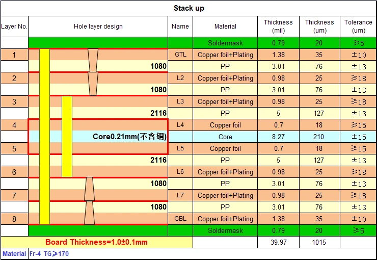
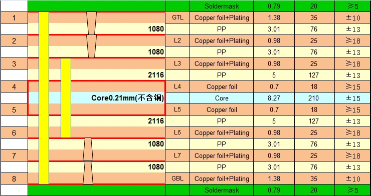
The full HDI stackup (2+4+2) at the start of the build. The board contains eight copper layers separated by 1080 / 1080+106 prepreg sheets, with a 0.21 mm copper-clad core at the center.
Stage 1: Cut (Steps 1–2)
Step 1 — Cut : The process starts with cutting large copper-clad laminates (typically 36″x48″, 40″x48″, or 42″x48″ panels) into smaller working panels. The CAM engineer first arranges the customer-supplied unit (single PCB design) into a set (multiple units + process borders), and then combines several sets into a panel (the actual manufacturing unit). Panel utilization is a key cost driver — better utilization means lower price per square meter.
Step 2 — Inner Layer : The inner copper layers (L2, L3, L6, L7 in the 2+4+2 stackup) are patterned using a photolithographic process. Dry film is laminated onto the copper surface, exposed through a phototool, and developed. Unexposed dry film is washed away, and the exposed copper is etched to leave the desired trace pattern. Minimum line width and spacing on the inner layers are typically 3 mil (0.076 mm) for HDI builds.
Stage 2: AOI, Oxidation & 1st Lamination (Steps 3–5)
Step 3 — Inner Layer AOI: Automated Optical Inspection scans every inner-layer trace for opens and shorts before lamination. Catching defects at this stage prevents expensive scrap later in the 8-layer 2-stage HDI PCB cycle.
Step 4 — Brown / Black Oxidation (Multibond): The inner-layer copper surfaces are chemically oxidized to form a micro-rough Cu2O / CuO layer. This dramatically increases the surface area and bond strength with the prepreg resin during lamination. Brown oxide (Cu2O-dominant) and black oxide (CuO-dominant) processes are both widely used in the industry.
Step 5 — 1st Lamination (压合): The four inner core layers (L3, L4, L5, L6) are stacked with prepreg sheets (typically 1080 or 1080+106) and outer copper foils, then pressed in a vacuum hydraulic press at around 180°C and 300–400 psi. After the first press, the panel is effectively a 4-layer sub-assembly with copper on both outer surfaces. The image below shows the cross-section right after the first lamination.
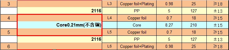
Cross-section after the 1st lamination. The 4-layer sub-assembly (L3–L4–L5–L6) is now ready for buried-via processing in the 8-layer 2-stage HDI PCB.
Stage 3: Buried Via Drilling & Plating (Steps 6–7)
Step 6 — Drill Buried Vias (钻埋孔): Mechanical drill bits (minimum 8 mil diameter) create the buried vias that connect the inner sub-assembly. For our 2+4+2 example, buried vias are drilled between L3 and L6 through the 4-layer core. Layout engineers must respect the “non-crossing” rule — you cannot have 3–5 and 4–6 buried vias in the same board because the drill paths would intersect. The image below shows the cross-section after buried-via drilling.
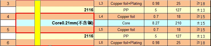
Cross-section after mechanical drilling of buried vias (L3–L6) in the 4-layer sub-assembly.
Step 7 — Plate Buried Vias (PTH): The drilled hole walls are metallized using a three-step process: desmear (removes epoxy smear), electroless copper deposition (creates a thin conductive seed layer), and electrolytic copper plating (builds up the barrel to 25 µm minimum). The aspect ratio (board thickness : hole diameter) is critical — exceed 10:1 and plating reliability drops sharply. Plating reliability is not the same thing as fill integrity, though: a barrel can plate cleanly and still hide a cavity, and the mechanisms behind those plating voids in microvias — hydrogen entrapment, additive imbalance and hole-wall preparation — are worked through in a separate guide.
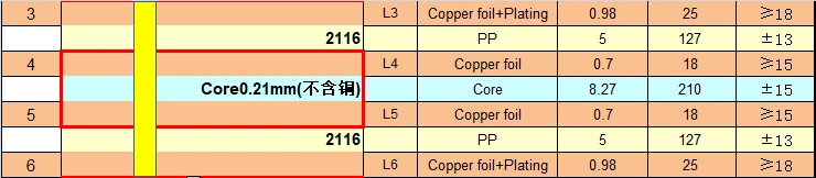
After electroless + electrolytic copper plating, the buried vias of the 8-layer 2-stage HDI PCB are fully metallized and electrically continuous.
Stage 4: Inner Layer 2 & 2nd Lamination (Steps 8–9)
Step 8 — Inner Layer 2: The buried vias are first resin-filled and planarized, then the second inner-layer pattern is imaged and etched. This produces the L2 and L7 copper layers, which will host the first set of microvias (micro blind vias) in the next stage.
Step 9 — 2nd Lamination: Two prepreg-copper-foil sandwiches are laminated onto the top and bottom of the 4-layer sub-assembly inside the 8-layer 2-stage HDI PCB. After this press, the panel is a 6-layer board with copper on both outer surfaces — the canvas for the first laser-drilling cycle.
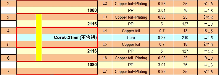
After the 2nd lamination, the panel is a 6-layer sub-assembly of the 8-layer 2-stage HDI PCB, with copper foil ready for the first laser-drilling step.
Stage 5: 1st Laser Drilling & Blind Via Plating (Steps 10–11)
Step 10 — 1st Laser Drilling (激光钻孔): CO2 or UV laser systems drill the first set of micro blind vias between L1–L2 and L7–L8. Typical micro-via diameter is 3–5 mil (0.076–0.127 mm) — far smaller than the 6 mil minimum of mechanical drilling. This is the defining capability that enables HDI PCB technology.
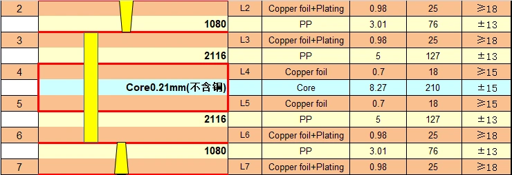
After the first laser-drilling step, micro blind vias (typically 0.1 mm diameter) connect L1–L2 and L7–L8.
Step 11 — 1st Blind Via Plating (电镀填孔): The microvias are metallized using the same electroless + electrolytic copper process. For stacked-via designs, the via is also filled with a special resin and capped with a planar copper layer — this prevents air entrapment and ensures reliable stacking for the next stage.
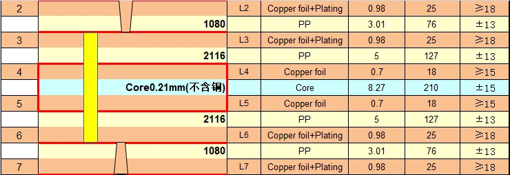
Cross-section of the 8-layer 2-stage HDI PCB after the first blind-via plating. The microvias are now electrically continuous to the next inner copper layer.
Stage 6: 3rd Lamination, 2nd Laser Drilling & Through-Holes (Steps 12–16)
Step 12 — Inner Layer 3: The outermost inner pattern (the L2/L7 sub-pattern) is re-imaged and etched if needed for the second HDI stage.
Step 13 — 3rd Lamination: The final two prepreg + copper-foil stacks are added to complete the 8-layer 2-stage HDI PCB construction. The panel is now a full 8-layer 2-Stage substrate with copper on the outermost surfaces.
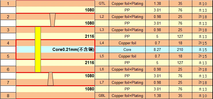
After the 3rd and final lamination, the 8-layer 2-stage HDI PCB reaches its full thickness of approximately 1.0 mm ± 0.10 mm.
Step 14 — 2nd Laser Drilling: A second laser cycle creates the L2–L3 and L6–L7 micro blind vias, completing the 2-stage HDI PCB via structure. The combination of staggered and stacked vias is now visible in cross-section.
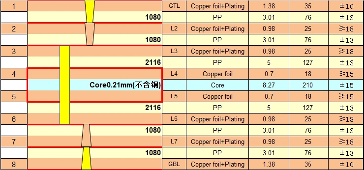
After the second laser-drilling cycle, the 8-layer 2-stage HDI PCB via stack is complete — each outer BGA pad is connected to the core through two sequential microvias.
Want to see the one-stage counterpart of this via stack? Our 4-layer 1-stage HDI irregular LED display PCB completes the same laser-microvia flow in a single sequential lamination cycle for P1.5625 fine-pitch LED screens.
Step 15 — Drill Through-Holes (钻通孔): Mechanical drilling creates the through-hole vias that connect all eight layers. These are typically used for power, ground, and signal paths that need to traverse the entire stack.
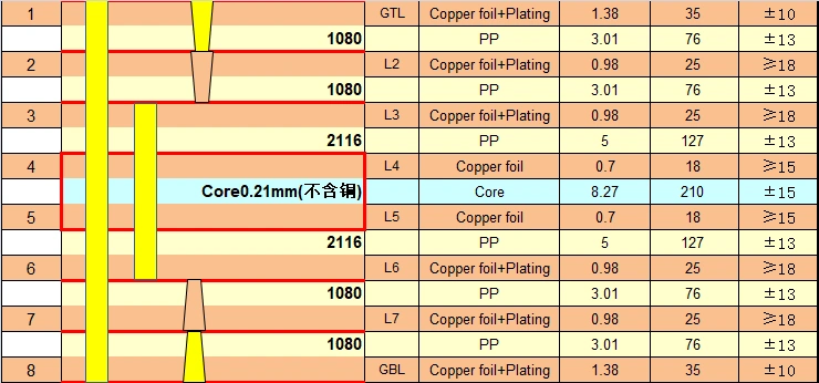
After mechanical drilling, the 8-layer 2-stage HDI PCB has both micro blind vias (laser) and through-hole vias (mechanical drill).
Step 16 — Final Plating (PTH): A second electroless + electrolytic copper plating cycle metallizes the through-hole barrels and microvias simultaneously, creating a fully connected 8-layer HDI PCB. Curious how blind, buried, and stacked microvias fit into different designs? Our HDI stackup and microvia guide compares the structures in detail.
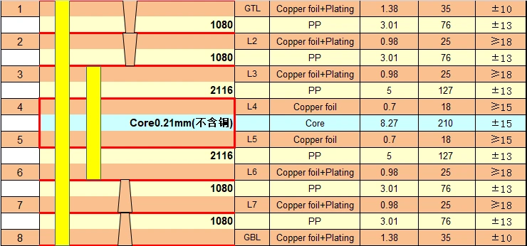
After the final plating step of the 8-layer 2-stage HDI PCB, all microvias and through-holes are fully metallized. The board is now electrically continuous across all 8 layers.
Stage 7: Outer Layer, Solder Mask, Finish & Ship (Steps 17–26)
Step 17 — Outer Layer Pattern Plating: The outermost copper layers (L1 and L8) are imaged, developed, and pattern-plated to form the final trace geometry, pads, and footprints. Trace width / spacing down to 2 mil (0.05 mm) is achievable on HDI PCB outer layers.
Step 18 — Outer Layer AOI: Another 100% optical inspection confirms the outer-layer pattern is defect-free before solder mask.
Step 19 — Solder Mask (阻焊): Liquid photoimageable solder mask (LPISM) is coated onto both surfaces, exposed through a phototool, and developed. The green (or black, red, blue) mask covers all areas except pads, vias, and silkscreen regions. A final thermal cure hardens the mask.
After solder mask application, the panel is recognizable as a finished 8-layer 2-stage HDI PCB — the green coating protects all non-solderable areas.
Step 20 — Legend (Silkscreen): Component reference designators, logos, and date codes are printed onto the solder mask using white or yellow epoxy ink.
Step 21 — Surface Finish: Exposed copper pads receive a surface finish to prevent oxidation and ensure solderability. Designs that use via-in-pad also go through a via filling and plugging step at this point, so the filled vias are planarized flush with the pads. The most common options are:
- ENIG (Electroless Nickel Immersion Gold) — the industry standard for HDI PCB; flat, lead-free, shelf life > 12 months.
- HASL (Hot Air Solder Leveling) — leaded or lead-free; excellent solderability but uneven surface for fine-pitch BGAs.
- OSP (Organic Solderability Preservative) — lowest cost, eco-friendly, but sensitive to handling.
- Immersion Silver / Tin — mid-cost options for specific applications.
Step 22 — Routing (鉸板): A CNC router or V-CUT machine separates the individual units (or sets) from the working panel. Outline tolerance, beveled edges, and slot dimensions are all controlled at this stage.
Step 23 — Electrical Test (E-Test): Flying-probe or bed-of-nails testers verify continuity (no opens) and isolation (no shorts) on every net. For 8-Layer 2-Stage HDI, this step is especially critical because any latent defect in the laser-via stack will be caught here.
Step 24 — Final Audit (终检): Cross-sectioning, solderability testing, ionic cleanliness testing, and visual inspection confirm the board meets IPC-6012 Class 2 or Class 3 requirements.
Step 25 — Packaging (包装): Each panel or unit is vacuum-sealed in a static-shielding bag with desiccant, and outer-carton labeling includes part number, batch, date code, and quantity.
Step 26 — Shipment (出货): Finished boards are shipped to the PCBA line for component assembly, or directly to the customer for further integration.
Key Takeaways: 8-Layer 2-Stage HDI PCB Build
- An 8-Layer 2-Stage HDI PCB requires 3 lamination cycles, 2 laser-drilling cycles, and 26 individual operations — far more than a standard 8-layer board.
- Buried vias must follow the non-crossing rule: 3–6 stacked vias are standard, but mixing 3–5 and 4–6 in the same design is not manufacturable.
- Staggered vias are easier and cheaper than stacked vias; reserve stacked vias for BGA escape routing on the most pin-dense components.
- Layout decisions made early in the design cycle have an outsized impact on yield — especially via stackup symmetry, copper balance, and micro-via aspect ratio. You can see the equipment behind every stage in our full PCB manufacturing capability overview.
High-density interconnect (HDI) PCB technology is the backbone of every modern compact electronic product — from 5G smartphones and AR/VR headsets to ADAS controllers and IoT sensors. Mastery of the 8-layer 2-stage HDI PCB process is what separates a “design that works” from a “design that ships at scale.”
From fine-pitch BGA fan-out to high-current power delivery, the 8-Layer 2-Stage HDI PCB stackup gives engineers the routing density and signal integrity they need — but only when the layout respects the process. If you are starting a new HDI PCB design, involve your PCB manufacturer in the stackup review before you commit Gerbers.
Conclusion: Building an 8-Layer 2-Stage HDI PCB
998PCB Group / Season Multilayer Circuit is a one-stop PCB and PCBA manufacturer with two decades of HDI PCB production experience. Our Shenzhen factory runs more than 20 HDI PCB production lines, capable of building 1-Stage, 2-Stage, 3-Stage, and any-layer HDI PCBs in volume — with full IPC-6012 Class 3 certification and US-based engineering support.
Need a custom stackup review for an 8-layer 2-stage HDI PCB, a manufacturability check on your Gerbers, or a quick-turn HDI PCB prototype? Visit our Contact Us page or send your files to our engineering team. We respond to every RFQ within one business day.
For more background on HDI PCB technology, see our What is an HDI PCB? guide and our 12-Layer 1-Stage HDI PCB product page. For the Chinese-language version of this manufacturing guide, visit our sister site 998pcb.com.
Ready to see this two-stage flow applied at higher density? Our 14-layer 2-stage HDI prototype PCB follows the same sequential lamination and double laser-drill sequence on a 2+10+2 stack — stacked 0.10 mm microvias, VIPPO via-in-pad for 0.2 mm BGA, and TDR-verified 100 ohm differential pairs.
Frequently Asked Questions About 8-Layer 2-Stage HDI PCB
Why does an 8-layer 2-stage HDI PCB need three lamination cycles?
An 8-layer 2-stage HDI PCB uses a 2+4+2 stackup built in three passes. The first cycle bonds the inner layers of the 4-layer core, the second adds the next inner-layer pair after the buried vias are drilled and plated, and the third bonds the outer copper foils in place. Each cycle must finish before the next drilling stage can reach the new layers, which is why a 2-stage build always costs three laminations.
What is the difference between blind vias and buried vias?
In an 8-layer 2-stage HDI PCB, buried vias connect only inner layers — in this build, between layers 3 and 6 — and are invisible from the outside of the finished board. Blind vias connect an outer layer to an adjacent inner layer (L1–L2 and L7–L8 here) and are laser-drilled from the surface after the corresponding lamination cycle.
Why are HDI microvias drilled by laser instead of mechanical bits?
Micro blind vias in an 8-layer 2-stage HDI PCB are typically 3–5 mil in diameter with a controlled depth, which is below the practical limit of mechanical drilling. A laser drills the small, precise holes needed for fine-pitch BGA fan-out without the wander and breakout a mechanical bit would produce at that size.
What is the non-crossing rule for buried vias?
In an 8-layer 2-stage HDI PCB, buried vias may not cross one another. In an 8-layer 2-stage design, 3–6 stacked vias are standard, but mixing 3–5 and 4–6 buried vias in the same board is not manufacturable because the crossing paths would tie the wrong layer pairs together. Staggering the vias avoids the problem and lowers cost at the same time.
When is via filling required in the HDI manufacturing process?
Via filling (plugging) is used for via-in-pad layouts and dense BGA escape routing, where the via must be filled with copper or epoxy and planarized flat. On this build it is performed after final plating and before the surface finish, so the filled vias sit flush under the component pads.
Does Season Multilayer Circuit manufacture 2-stage HDI in volume?
Yes. 1-Stage to 4-Stage HDI structures are in regular volume production; any-layer HDI is currently offered at prototyping level. The 8-layer 2-stage process described in this guide is one of our standard volume builds, and our engineering team can review your stackup before you commit Gerbers.
Planning an HDI build? See how Season PCB’s HDI PCB manufacturing services support up to 5-stage stackups.