Book Appointment Now

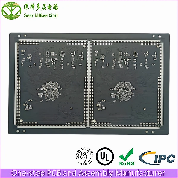
8-Layer PCB Core Board Samples
Accelerate your hardware validation with industry-grade 8-layer PCB prototypes. Built for complex multilayer architectures, rigorous thermal stability, and flawless signal integrity — delivered in as fast as 72 hours.
When your design demands more than a 4‑layer or 6‑layer board can deliver, an 8‑layer core PCB sample is the fastest path from concept to validated hardware. Balance stackup architecture, ±8% impedance control, and zero‑defect testing — so your engineering team can iterate with confidence and hit your product launch deadline.
✓ 5–7 Day Quick-Turn — sample batches shipped in under a week
✓ No MOQ — validate your design from a single piece
✓ Free DFM Check — stackup and impedance review before production
✓ ±8% Impedance Control — TDR verified with Polar Instruments

8
Layer Count
2.9/3 mil
Min. Trace / Space
0.20 mm
Min. Via Diameter
Tg 155
Glass Transition Temp
1 µ”
ENIG Gold Thickness
ISO 9001:2015
ISO 14001
UL (E305905)
IPC Class 2 / Class 3
IATF 16949
RoHS
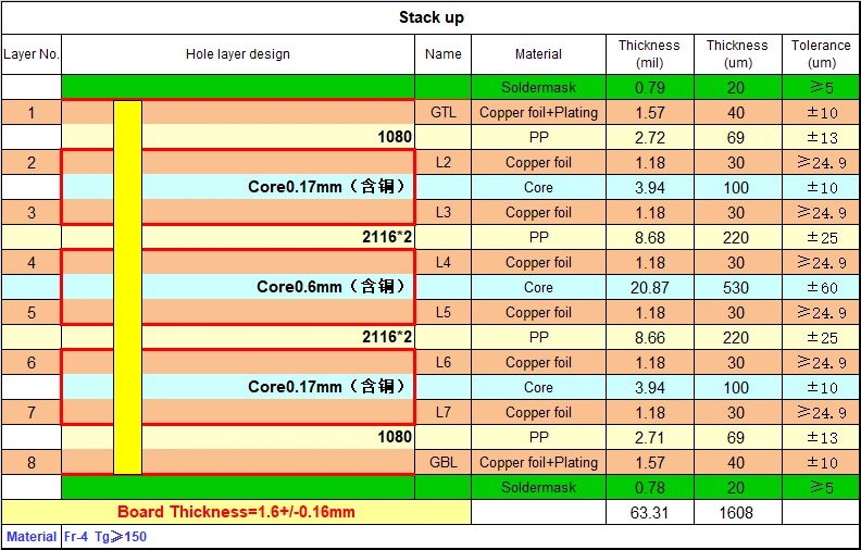
8-Layer Core PCB Stackup Configuration
To ensure perfect structural symmetry and prevent board warping during reflow soldering, we utilize a balanced 8-layer core construction. Below is our standard high-reliability layout:
- Layer 1 (Top): Signal Layer — Main high-speed trace routing and component placement. (1.57 mil, 1/3oz + Plating)
- Layer 2: Ground Plane (GND) — Critical reference shield for Top Layer signals. (1.18mil, 1 oz)
- Layer 3: Inner Signal 1 — Controlled impedance routing for internal buses. (1.18mil, 1oz)
- Layer 4: Power Plane (PWR) — Dedicated low-impedance power distribution. (1.18mil, 1oz)
- Layer 5: Ground Plane (GND) — Power isolation and inner signal reference. (1.18mil, 1oz)
- Layer 6: Inner Signal 2 — Auxiliary internal routing. (1.18mil, 1oz)
- Layer 7: Power / Ground Plane — Configurable according to power net complexity. (1.18mil, 1oz)
- Layer 8 (Bottom): Signal Layer — Bottom routing and secondary components. (1.57mil, 1/3 oz + Plating)
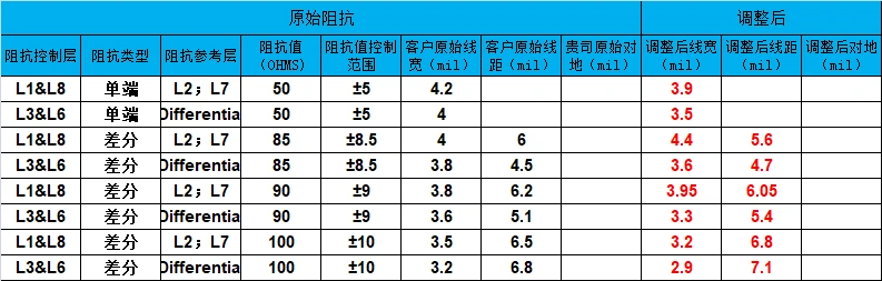
If your original design does not meet the strict impedance requirements, don’t worry. Our engineering team will optimize it for you. The diagram below illustrates how we adjust the impedance traces on this 6-layer optical module PCB:
Technical Specifications for 8-Layer Core PCB Samples
| Parameter | Specification | Advanced Capabilities |
|---|---|---|
| Layer Count | 8 Layer | 2–32L (mass); 2–64L (sample) |
| Base Material | FR-4 S1000H Tg 155 | SY, NY, TUC, ZY, EMC, KB, ITEQ, Rogers, Megtron, Nelco, Isola |
| Board Thickness | 1.6mm | 0.2–6.4mm (mass); 0.15–20mm (sample) |
| Panel Size | 129.2 × 82.6mm / 2-up | 800 × 600mm (mass); 1050 × 610mm (sample) |
| Copper Thickness | Outer: 1 oz Inner: 1 oz | Outer: 1/3–12 oz Inner: 1/4–12 oz |
| Min Drill Size | 0.2mm | 0.15mm (mass); 0.127mm (sample) |
| Min Trace Width/Spacing | 2.9/3 mil | 2.5/2.5 mil (1 oz) 2/2 mil (0.5 oz) |
| Min BGA Pad | 0.25mm | 0.15mm |
| Surface Finish | ENIG 1–2 µ” | OSP, ENIG, HASL, Electric Hard Gold, ENIG+OSP, ENEPIG, Immersion Silver & Tin |
| Specialized Processes | Half holes | Resin Plugged Vias, Copper Paste Via Filling, Copper Plating Via Filling, POFV |
| Solder Mask Color | Matte Black | Green, Blue, Black, White, Yellow, Red, Purple, Matte Green, Matte Blue, Matte Black |
| Impedance Control | ±10% (50/85/90/100Ω) | ±8% (Tight Tolerance) ±5% (Strict Tolerance) |
| Min Routing Tolerance | ±0.15mm | ±0.075mm |
| Quality Standard | IPC Class 2, RoHS | IPC Class 3, UL, RoHS, IATF 16949, GJB |
| PCB Type | Multilayer | HDI, Multilayer, Rigid-Flex, High Frequency, High Speed, Hybrids & Mixed Dielectrics |
Why Upgrade to an 8-Layer PCB?
When standard 4-layer or 6-layer PCBs hit their physical limits regarding electromagnetic interference (EMI) and cross-talk, upgrading to an 8-layer PCB architecture becomes essential. Our 8-layer core PCB samples provide the perfect foundation for high-density interconnect (HDI) designs, high-speed digital buses, and complex RF circuits.
Enhanced EMI Shielding
Four dedicated routing layers interleaved with four solid ground/power planes provide exceptional return-path control, minimizing radiation and cross-talk in dense layouts.
Impedance Stability
Rigid core integration ensures ultra-stable dielectric thickness, meeting tight differential signaling requirements for PCIe, DDR4/DDR5, USB 3.0, and 10G/40G Ethernet.
Optimal Thermal Management
Multiple heavy internal copper planes act as built-in heat sinks for high-power processors, FPGAs, and AI accelerator chips, preventing thermal throttling during sustained workloads.
Design Flexibility
The configurable Layer 7 plane (power or ground) gives designers the freedom to optimize power distribution networks without sacrificing signal integrity.
6-Layer vs 8-Layer PCB: Which One Does Your Design Need?
Layer count is a routing-density decision, not a prestige decision. Adding layers costs money; adding too few layers costs respins. Use the criteria below to pick the smallest stackup that still meets your signal-integrity and EMI targets.
A 6-layer board is usually enough when your design has a single high-speed interface, a BGA pitch of 0.8mm or coarser, and no supply rail that needs its own dedicated plane. A typical 6-layer build (signal – ground – signal – signal – power – signal) handles DDR3/DDR4, USB 3.0 and Gigabit Ethernet at ±10% impedance control without difficulty.
Move up to an 8-layer core PCB when any of the following applies: two or more independent high-speed buses share the board (PCIe Gen4 alongside 10G Ethernet, for example); the package is a fine-pitch BGA of 0.65mm or below, so escape routing needs an extra signal layer; several supply rails each want their own plane for power integrity; or EMI compliance is a hard requirement and every trace needs a solid return path directly beneath it. The core construction adds a second dedicated ground plane and a configurable power plane while holding the board at the 1.6mm industry-standard thickness.
Both stackups run on the same quick-turn line, so you can validate a 6-layer prototype and step up to 8 layers without changing supplier or process. Upload your Gerber files and our CAM engineers will confirm which build meets your impedance and EMI targets — or review our fast PCB manufacturing services for expedited schedules.
Key Industries & Applications
Our 8-layer PCB solutions are engineered to meet the stringent requirements of mission-critical industries. By balancing signal integrity, thermal management, and compact footprint, our boards empower high-performance hardware across the following sectors:
Networking & Communication
High-speed routers, enterprise switches, and server backplanes requiring stable 100Ω differential signaling for 10G/40G Ethernet.
Automotive Electronics
ADAS, infotainment consoles, and sensor fusion modules demanding IATF 16949 compliance and harsh-environment durability.
Industrial Automation
High-precision PLC controllers, robotics controllers, and automated manufacturing sensor arrays operating 24/7 in electrically noisy factory environments.
AI & High-Performance Computing
AI training hardware, server motherboards, and edge computing nodes requiring dense routing and heavy power delivery for GPU/TPU modules.
Medical Devices
Diagnostic imaging equipment and patient monitoring systems that require reliable signal integrity and strict quality standards.
Aerospace & Defense
Avionics communication modules and radar signal processing boards demanding IPC Class 3 reliability and zero-defect manufacturing.

Why Choose Season PCB for 8-Layer Core Prototypes
We combine advanced manufacturing capabilities with strict quality management to ensure your 8-layer designs perform under pressure.
High-Speed Signal Integrity
Controlled impedance with ±8% standard and ±5% advanced tolerance for 50Ω, 85Ω, 90Ω, and 100Ω differential pairs.
Advanced Material Selection
High-Tg FR-4 (Tg 150/Tg 170/Tg 180), Rogers, Megtron, and Isola laminates for superior electrical and thermal performance.
HDI Capabilities
Laser-drilled microvias (blind & buried), stacked/staggered via structures, and any-layer interconnect designs.
Specialized Processes
Resin plugged vias, copper paste via filling, POFV (Plated Over Filled Via), and back drilling for signal integrity optimization.
Free DFM Checking
CAM engineers review every Gerber file for manufacturability before production, catching design issues early and saving you costly re-spins.
No Minimum Order Quantity
From 1 prototype to 100,000+ mass production units — we support your entire product lifecycle with one manufacturing partner.
Zero-Defect Guarantee — Multi-Stage Inspection
Prototyping is expensive — a single defective sample costs you a full design iteration cycle. We eliminate defects before they ship with rigorous multi-stage inspection protocols:
100% Automated Optical Inspection
Scans all 8 layers post-etching to eliminate inner-layer opens, shorts, or registration errors before lamination.
Flying Probe Electrical Testing
Ensures 100% netlist continuity tracking against your original Gerber files — every net is verified.
TDR Impedance Verification
Validates exact ohm ratings of differential pairs using Polar Instruments test equipment with a full test report.
Solderability & Thermal Shock Testing
Guarantees structural interlayer adhesion, preventing delamination during manual or automated assembly.
Our 8-layer PCB core samples are built for designs that have outgrown 4-layer and 6-layer routing. The capability set covers controlled-impedance routing, fine-line traces, tight layer-to-layer registration and 100% electrical test before shipment. See the full PCB manufacturing capability list for the process envelope.
For reliable production, contact Season PCB. We offer fast turnaround with no MOQ requirement, and for volume programmes the same stackups run on 998PCB Group’s 2–30 layer PCB lines. Upload your Gerber files any time for a DFM review.
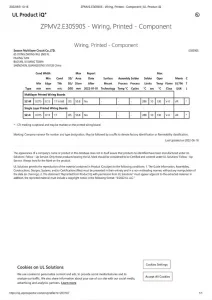
Manufacturing follows IPC-6012 qualification standards for multilayer boards, and every board is accepted to IPC-A-600 criteria. UL recognition for laminate materials is held under E-File E305905 — more background in our guide to UL certified PCB standards.
Certifications & Compliance
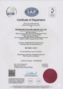
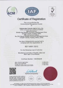
Our 8-layer core PCB production is backed by third-party certification: ISO 9001:2015 quality management, ISO 14001 environmental management, and UL recognition for laminate materials (E-File E305905). IATF 16949, RoHS and GJB compliance documentation is available with your order.
Frequently Asked Questions
Q1: What is the typical lead time for a quick-turn 8-layer PCB sample?
A: Our standard lead time for an 8-layer core sample batch is 5 to 7 working days. For urgent engineering verifications, we offer an expedited express service that delivers fabricated boards within 72 to 94 hours depending on design complexity. Timelines by layer count and surface finish are listed in our PCB lead time guide.
Q2: How do you ensure layer-to-layer alignment symmetry in an 8-layer board?
A: We use state-of-the-art LDI-guided automated pinless pinning systems during the pre-preg and core lamination processes. This limits inner-layer registration offsets to less than ±1 mil (±25.4 µm).
Q3: Can I mix different core materials in my 8-layer stackup?
A: Yes, we support hybrid stackups (e.g., Rogers layers combined with standard FR4 cores) specifically engineered for high-frequency RF sections integrated onto a digital base board.
Q4: Do you provide impedance test reports with 8-layer PCB samples?
A: Yes. Every 8-layer sample batch includes TDR (Time Domain Reflectometry) impedance verification with a full test report documenting compliance with your specified impedance values (50Ω, 85Ω, 90Ω, or 100Ω). We use Polar Instruments test equipment for maximum accuracy.
Q5: Do you offer ENIG surface finish for 8-layer boards?
A: Yes, ENIG (Electroless Nickel Immersion Gold) 1–2 µ” is our standard surface finish for 8-layer PCBs. We also offer OSP, HASL, Electric Hard Gold, ENIG+OSP, ENEPIG, Immersion Silver, and Immersion Tin — contact our team to discuss which finish is optimal for your application.
Q6: What drives the price of an 8-layer core PCB sample?
A: The dominant cost drivers are layer count and stackup symmetry, panel utilisation and board outline size, laminate grade (standard FR-4 versus low-loss or high-Tg material), copper weight, surface finish, impedance tolerance class (±10%, ±8% or ±5%), order quantity and schedule. A standard Tg 155 FR-4 build at ±10% sits at the entry point, while tight-tolerance impedance control and expedited schedules add cost. Our guide to the components of PCB prices breaks each factor down.
Ready to Prototype Your 8-Layer Core Design?
Upload your Gerber files (RS-274X or ODB++ format) for an instant PCB quote. Our CAM engineers will run a complimentary DFM check and deliver a competitive quotation within 24 hours.
Tel: (+86) 18681528532 (WhatsApp)
E-mail: roc@season-pcb.com