Book Appointment Now

What is an HDI PCB?
I. Overview of HDI PCBs
Definition of HDI PCBs (What is an HDI PCB?)
What is an HDI PCB? A High-Density Interconnect (HDI) PCB is a type of circuit board manufactured using micro-blind vias and buried via technology to achieve a higher wiring density. As technology advances, electronic devices demand higher signal transmission speeds, requiring PCBs to provide impedance control for alternating current characteristics, high-frequency transmission capabilities, and reduced electromagnetic interference (EMI). To meet these requirements, stripline and microstrip structures are employed, necessitating multilayer designs. To minimize signal integrity issues, low dielectric constant and low attenuation insulating materials are used. Additionally, to accommodate the miniaturization and array-based packaging of electronic components, PCB density continues to increase. HDI PCBs adopt a modular parallel design, with each module offering 1000VA capacity (1U height) and natural cooling. Up to six modules can be integrated into a 19″ rack. Leveraging fully digital signal processing (DSP) technology and patented innovations, these products deliver broad load adaptability and robust short-term overload tolerance, independent of load power factors or peak coefficients.
Evolution of HDI PCBs
Traditional PCB drilling faces limitations due to drill bit constraints, with costs escalating sharply for hole diameters below 0.15mm. HDI technology replaces mechanical drilling with laser drilling (hence the term “laser board”). HDI boards typically feature 3-5 mil (0.076-0.127mm) laser-drilled vias and 2-4 mil (0.05-0.10mm) trace widths, enabling smaller pad sizes and higher wiring density per unit area—the hallmark of high-density interconnects.
HDI technology has driven PCB industry advancements, allowing dense arrangements of BGA, QFN, and other components. Today, 1-Stage HDI is widely used in PCBs with 0.5-pitch BGAs. The synergy between HDI and chip technologies continues to push both fields forward.
II. HDI Stage Classification and Common Stackup Structures
HDI stackups and costs vary depending on design, even for boards of the same stage. For example, a 6-layer 1-Stage HDI can adopt:
- Single lamination with blind vias
- Double lamination with blind/buried vias
- Double lamination (standard HDI)
Below, we explain different HDI stages, their cost implications, production timelines, and efficiency to guide PCB layout engineers in design optimization.
1-Stage HDI Structure: 1+N+1
(Standard 6-layer 1-Stage HDI : 2 laminations, 1 laser drill)
Standard 6-layer 1-Stage HDI (highest cost): Combines blind, buried, and through-hole vias. Requires 2 laminations, 1 laser drill, 1 buried via plating, and 1 blind/through-hole plating.
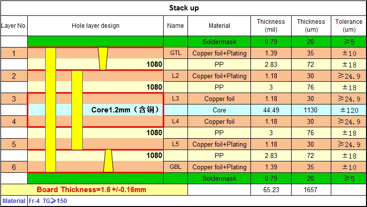
6-layer 1-Stage Blind Via HDI (lowest cost): Uses 1 lamination and 1 plating step for through-holes and blind vias. Eliminates buried via drilling, plating, and resin filling, reducing costs and improving efficiency.
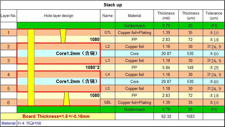
Simplified 6-layer 1-Stage HDI: Removes through-holes, reducing drilling costs. Offers shorter lead times and lower costs compared to standard structures.
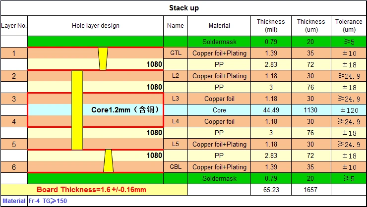
2-Stage HDI Structure: 2+N+2
Standard 6-layer 2-Stage HDI: 2 laminations, 2 laser drills
Standard 6-layer 2-Stage HDI (highest cost): Uses staggered (e.g., 1-2, 2-3 layers) or stacked blind vias (e.g., 4-5, 5-6 layers). Stacked vias require precise via filling to avoid open circuits. Involves 2 laminations, 2 laser drills, 1 buried via plating, and 2 blind via platings.
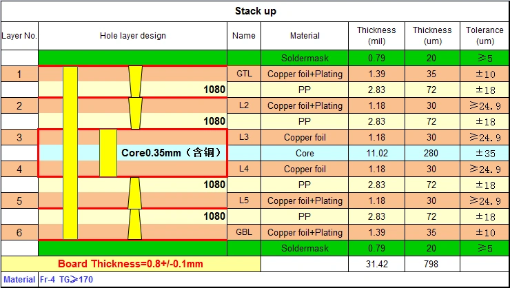
6-layer 2-Stage Blind Via HDI: Eliminates buried vias, reducing drilling and resin-filling costs. Recommended for cost-sensitive designs.
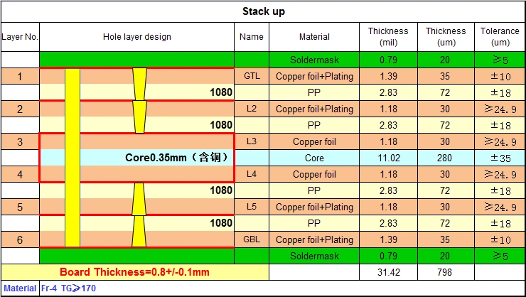
Blind/Buried Via 6-layer 2-Stage HDI: Skips through-holes (e.g., L2-5 buried vias). Combines plating steps for buried and blind vias, lowering costs and cycle times.
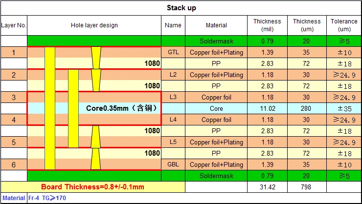
Simplified 6-layer 2-Stage HDI: Optimizes via placement (e.g., L2-5 instead of L3-4) to reduce plating steps and improve yield.
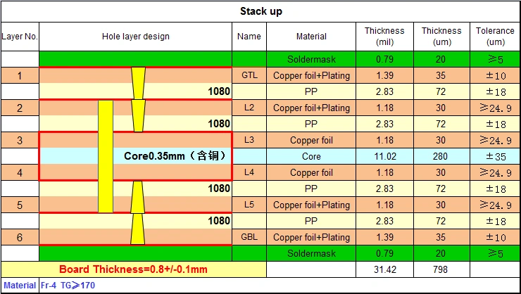
3-Stage HDI Structure: 3+N+3
(Standard 8-layer 3-Stage HDI: 3 laminations, 3 laser drills)
For example, an 8-layer 3-Stage HDI requires three laminations and three laser drills. Engineers are encouraged to innovate simpler, cost-effective designs based on standard stackups.
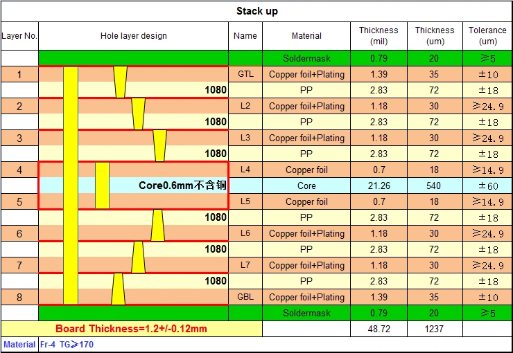
4-Stage HDI Structure: 4+N+4
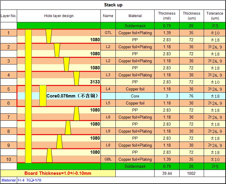
(Standard 10-layer 4-Stage HDI: 4 laminations, 4 laser drills)
A 10-layer 4-Stage HDI reference stackup is provided. Contact Season Multilayer Circuit for customized solutions.
Any-Layer HDI
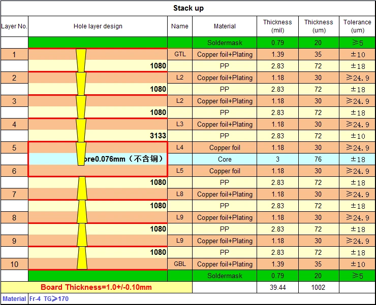
Any-layer HDI uses laser-drilled blind vias from the core outward, enabling unrestricted layer-to-layer interconnects. Stacked vias require precise laser depth control (interlayer thickness ≤4 mil), limiting board thickness (e.g., ~1.0mm for 10 layers). Due to stringent process requirements (e.g., via filling, alignment), any-layer HDI is currently limited to prototyping at Season Multilayer Circuit, with mass production under development.
Key Takeaways
- Laser drills per stage: 1-Stage (1 drill), 2-Stage (2 drills), etc.
- Any-layer HDI starts laser drilling from the core, with one lamination per drill.
HDI technology enables miniaturization while meeting high-performance demands. Widely used in smartphones, laptops, automotive electronics, and 4G/5G modules, HDI adoption grows with advanced chipsets.
From 0.5-pitch BGAs to multi-signal I/O layouts, 1-Stage HDI is increasingly insufficient. 2-Stage+ HDI (stacked/staggered vias) is now the focus for R&D teams and manufacturers.
Conclusion
Season Multilayer Circuit specializes in advanced HDI and multilayer PCB manufacturing, offering global clients one-stop PCB/PCBA solutions. For technical support or customized designs, contact our team. Your needs drive our innovation—reach out today!
Visit our Process Capabilities page for additional details.
For more information on HDI PCB technology, visit the IPC standards website, which provides detailed specifications for HDI PCB design and manufacturing. The IEEE also publishes technical papers on HDI PCB applications in modern electronics.