Book Appointment Now

Precision-Engineered 8-Layer Core PCB Samples
Accelerate your hardware validation with industry-grade 8-layer prototypes. Built for complex multilayer architectures, rigorous thermal stability, and flawless signal integrity.
- ISO 9001 & ISO 14001 Certified Factory
- IATF 16949 Automotive Quality Standard
- UL & Rohs Certified


Standard 6-Layer PCB Stackup for Optical Transceivers
A well-designed stackup is crucial for electromagnetic compatibility (EMC) and power integrity (PI). Here is our recommended high-speed 6-layer stackup configuration:
- Layer 1 (Top): Signal Layer — Main high-speed trace routing and component placement. (1.57 mil, 1/3oz + Plating)
- Layer 2: Ground Plane (GND) — Critical reference shield for Top Layer signals. (1.18mil, 1 oz)
- Layer 3: Inner Signal 1 — Controlled impedance routing for internal buses. (1.18mil, 1oz)
- Layer 4: Power Plane (PWR) — Dedicated low-impedance power distribution. (1.18mil, 1oz)
- Layer 5: Ground Plane (GND) — Power isolation and inner signal reference. (1.18mil, 1oz)
- Layer 6: Inner Signal 2 — Auxiliary internal routing. (1.18mil, 1oz)
- Layer 7: Power / Ground Plane — Configurable according to power net complexity. (1.18mil, 1oz)
- Layer 8 (Bottom): Signal Layer — Bottom routing and secondary components. (1.57mil, 1/3 oz + Plating)
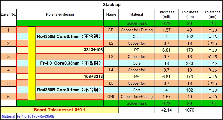
If your original design does not meet the strict impedance requirements, don’t worry. Our engineering team will optimize it for you. The diagram below illustrates how we adjust the impedance traces on this 6-layer optical module PCB:
