Book Appointment Now

High-Performance 6-Layer PCB for Optical Modules
Engineered for High-Speed Data Transmission, Strict Impedance Control, and Compact Form Factors (SFP/QSFP/OSFP).
- ISO 9001 & ISO 14001 Certified Factory
- IATF 16949 Automotive Quality Standard
- UL & Rohs Certified
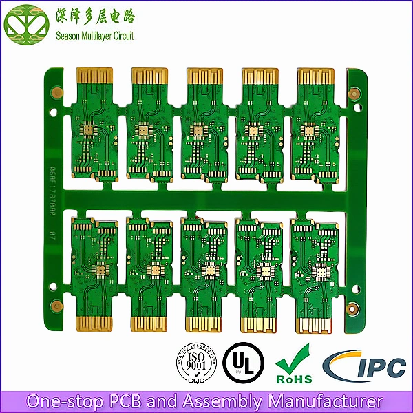
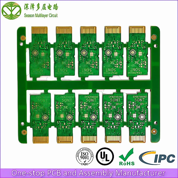
Standard 6-Layer PCB Stackup for Optical Transceivers
A well-designed stackup is crucial for electromagnetic compatibility (EMC) and power integrity (PI). Here is our recommended high-speed 6-layer stackup configuration:
- Layer 1 (Top) – Signal (Component): Used for high-speed differential pairs and component placement. The typical thickness is 1.57 mil (H oz + Plating).
- Layer 2 – Ground (GND): Serves as the reference plane for Layer 1 and provides EMI shielding. The typical thickness is 0.7 mil (H oz).
- Layer 3 – Inner Signal / Routing: Dedicated to low-speed signals and control lines. The typical thickness is 0.7 mil (H oz).
- Layer 4 – Power (PWR) / GND: Configured for the power distribution network (PDN). The typical thickness is 0.7 mil (H oz).
- Layer 5 – Ground (GND): Serves as the reference plane for Layer 6. The typical thickness is 0.7 mil (H oz).
- Layer 6 (Bottom) – Signal (Gold Finger): Used for edge connector routing (gold fingers) and auxiliary components. The typical thickness is 1.57 mil (H oz + Plating).
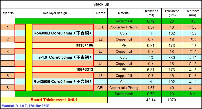
If your original design does not meet the strict impedance requirements, don’t worry. Our engineering team will optimize it for you. The diagram below illustrates how we adjust the impedance traces on this 6-layer optical module PCB:

Overcoming the Challenges of High-Speed Optical Transceiver PCBs
Optical modules require ultra-high reliability in extremely confined spaces. Traditional PCBs often fail to meet the stringent signal integrity and thermal demands of 25G, 100G, or 400G data rates. Our tailored 6-layer PCB solutions solve these critical bottlenecks:
- Signal Degradation: We utilize advanced high-speed, low-loss materials (e.g., Rogers, Megtron 6) to ensure minimal insertion loss.
- Impedance Mismatch: Strict ±10%(or±5% upon request) controlled impedance for differential pairs and single-ended lines.
- Thermal Dissipation: Integrated thermal vias and heavy copper options to effectively dissipate heat from lasers (EML/DFB) and ICs.
Technical Specifications & Capabilities for Optical PCBs
- Base Material: High-Tg FR4, Rogers, Nelco, Panasonic Megtron 6 / Megtron 7.
- Layer Count: Dedicated 6-layer lines (Scalable up to 32 layers for high-tier OSFP).
- Surface Finish: ENIG (Electroless Nickel Immersion Gold) & Hard Gold Plating (≥30U) for Gold Fingers to withstand repetitive insertions.
- Min. Trace Width/Spacing: 2.5/2.5 mil (0.0635mm).
- Min. Laser Via Size (HDI): 3 mil (0.075mm) for blind vias configuration.
- Impedance Tolerance: ±10% (Standard), ±5% (Precision).
Supported Optical Module Form Factors
Our 6-layer PCBs are widely implemented in various optical communication standards:
- SFP+ / SFP28: For 10G/25G Ethernet and Storage Area Networks.
- QSFP+ / QSFP28: Ideal for 40G/100G data center interconnects.
- CFP/CFP2/CFP4: Designed for long-haul coherent optical transport.
- Active Optical Cables (AOC): High-density layouts for short-range high-speed cabling.
Rigorous Testing for 100% Reliability
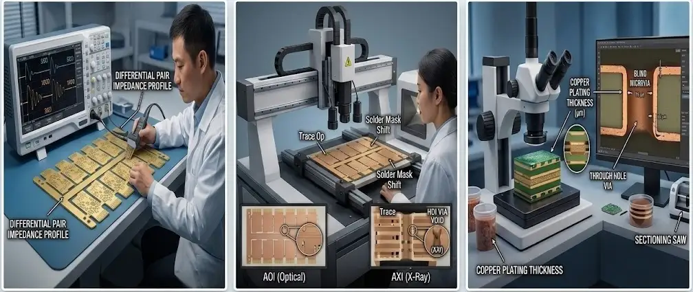
- TDR Testing (Time Domain Reflectometry): Validates precise impedance control along the high-speed traces.
- AOI & Automated X-Ray Inspection: Detects inner layer shifts and solder joint voids in HDI vias.
- Microsectioning Analysis: Verifies copper plating thickness in through-holes and blind vias.
- Flying Probe / Universal Electrical Test: Ensures 100% continuity and no short circuits.
Frequently Asked Questions
Q1: Why is a 6-layer PCB preferred over a 4-layer PCB for optical modules?
A: A 6-layer PCB provides dedicated ground and power planes, which are essential for isolating high-speed TX/RX differential lines. This significantly reduces crosstalk, improves EMI performance, and provides cleaner power delivery (PDN) compared to a 4-layer board.
Q2: What surface finish is best for the gold fingers of an optical module PCB?
A: Hard Gold Plating (typically 30u” or thicker) over Nickel is highly recommended for the edge connector (gold fingers) to ensure wear resistance over hundreds of insertion cycles. The rest of the board usually utilizes ENIG for excellent solderability.
Q3: How do you guarantee the ±10% impedance control for high-speed differential pairs?
A: We use polar instruments for pre-layout stackup simulation and run TDR (Time Domain Reflectometry) tests on every batch of coupons or boards to ensure actual values match the design specifications.
Ready to Launch Your Next Optical Module Project?
Get expert DFM (Design for Manufacturing) feedback and a competitive quote within 24 hours.