Book Appointment Now

Advanced 10-Layer M.2 SSD PCB Manufacturing
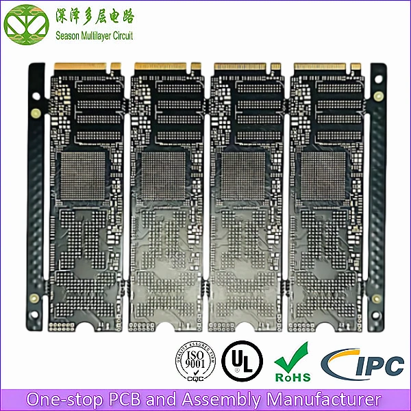
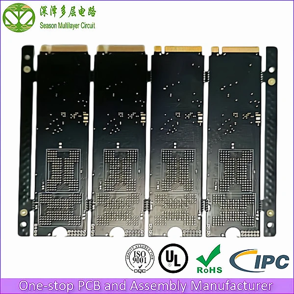
Engineered for next-generation NVMe PCIe solid-state drives. Our 10-layer M.2 SSD PCB delivers exceptional signal integrity at 0.85mm board thickness, supporting SMI, Phison, and Silicon Motion controller platforms for laptops, Mini PCs, ultrabooks, and gaming consoles.
✓ Ultra-Thin
✓ 2.5mil Trace & Space
✓ Electric Gold Finger 15U”
✓ Resin Plug Via
✓ 24h DFM Review
✓ Turnkey PCBA
10
Layer Count
2.5/2.5 mil
Min. Trace / Space
0.20 mm
Min. Via Diameter
Tg 180
Glass Transition Temp
1 µ”+15 µ”
ENIG +Electric Gold Finger
ISO9001-2004
ISO14001
UL (E305905)
IPC-Class 2/Class 3
IATF 16949
RoHS
10-Layer M.2 SSD PCB Stackup Diagram
This proven 10-layer stackup architecture dedicates dedicated ground and power planes adjacent to each signal layer, minimizing crosstalk, ensuring clean return paths, and maintaining tight impedance control for PCIe Gen3/Gen4/Gen5 differential pairs running at multi-gigabit data rates.
- L1 (Top) – Signal: Component placement, high-speed traces. The typical thickness is 1.4 mil (1/3 oz + Plating).
- Layer 2 – Ground (GND): Reference plane for L1 signals. The typical thickness is 0.7 mil (H oz).
- Layer 3 – Inner Signal : High-speed routing (PCIe lanes). The typical thickness is 0.7 mil (H oz).
- Layer 4 – PWR Plane: Power distribution (VCC, VCCQ). The typical thickness is 0.7 mil (H oz).
- Layer 5 – Ground (GND): Isolation & return path. The typical thickness is 0.7 mil (H oz).
- Layer 6 – Inner Signal : NAND flash interface routing.The typical thickness is 0.7 mil (H oz).
- Layer 7 – PWR Plane : Auxiliary power rails.The typical thickness is 0.7 mil (H oz).
- Layer 8 – Inner Signal : Bottom-side routing & DRAM interface.The typical thickness is 0.7 mil (H oz).
- Layer 9 – Ground (GND): Bottom-side routing & DRAM interface.The typical thickness is 0.7 mil (H oz).
- Layer 10 (Bottom) – Signal : Bottom component pads & connector. The typical thickness is 1.4 mil (1/3 oz + Plating).
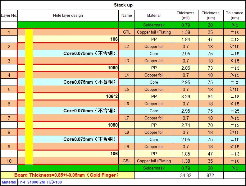
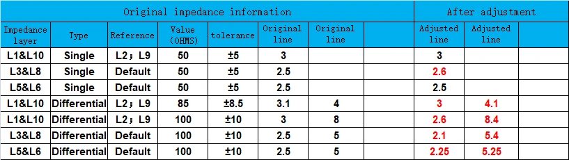
💡 Custom Stackup Optimization: If your existing design cannot meet stringent impedance requirements, our engineering team provides pre-production stackup optimization — adjusting dielectric thicknesses, copper weights, and material selections to hit your target impedance values. All stackups are validated using Polar CITS800s simulation before fabrication.
Technical Specifications & Manufacturing Capabilities
Every specification below reflects our proven mass-production capability, not just laboratory limits. Values marked “Sample capability” represent our advanced quick-turn prototyping tier.
| Parameter | Specification | Advanced Capabilities |
| Layer Count | 10Layer | 2-32L(Mass); 2-64L(Sample) |
| Base Material | Fr-4.0 S1000-2M Tg180 | SY, NY,TUC,ZY,EMC,KB,ITEQ, Rogers, Megtron , Nelco,Isola |
| Board Thickness | 0.85mm±0.05 | 0.2-6.4mm(Mass);0.15-20mm(Sample) |
| Panel Size | 106*80mm/4 | 800*600mm(Mass);1050*610(Sample) |
| Copper Thickness | Outer: 1 OZ Inner: H OZ | Outer: 1/3-12 OZ Inner: 1/4-12 OZ |
| Min Drill Size | 0.2mm | 0.15mm(Mass);0.127mm(Sample) |
| Min Trace Width/Spacing | 2.5/2.5mil | 2.5/2.5mil(1OZ) 2/2mil(HOZ) |
| Min BGA Pad | 0.25 | 0.15mm |
| Surface Finish | ENIG 1U”+Electric Hard Gold 15U” | OSP,ENIG,HASL,Electric Hard Gold, ENIG+OSP,ENEPIG,mmersion Silver & Tin |
| pecialized Processes | POFV | Resin Plugged Vias,Copper Paste Via Filling, Copper Plating Via Filling |
| Solder Mask Color | Matte Black | Green, Blue,Black,White,Yellow,Red,Purple, Matte Green,Matte Blue,Matte Black |
| Impedance Control | ±10% (50/85/100Ω) | ±5% (Strict Tolerance) |
| Min Routing Tolerance | ±0.10mm | ±0.75mm |
| Quality Standard | IPC-Class 2 ,RoHS | IPC-Class 3,UL,Rohs,IATF16949,GJB |
| PCB Type | Multilayer | HDI,Multilayer,Rigid-Flex,High Frequency,High Speed,Hybrids & Mixed Dielectrics |
High-Density 10-Layer M.2 SSD PCB — Built for Speed, Reliability & Scale
The 10-layer M.2 SSD PCB from Season PCB (Season Multilayer Circuit) is a high-density multilayer printed circuit board specifically engineered for next-generation NVMe PCIe solid-state drives. Leveraging 2.5mil trace/space precision, a 0.85mm ultra-thin profile, and rigorous impedance control across 10 conductive layers, this board delivers the signal integrity, thermal stability, and manufacturing consistency demanded by tier-1 SSD brands and OEMs worldwide.
Designed around SMI (Silicon Motion), Phison, Marvell, and InnoGrit controller platforms, the board supports PCIe Gen3/Gen4/Gen5 NVMe protocols across M.2 2280, 2242, 2260, U.2, and mSATA form factors. Since 2016, Season PCB has been one of China’s first manufacturers to achieve mass-production yields on sub-3mil geometry 10-layer SSD boards — and we’ve been refining the process every year since.
What Makes This 10-Layer M.2 SSD PCB Exceptional
📏
0.85mm Ultra-Thin Profile
47% thinner than a standard 1.60mm 10-layer board. Fits seamlessly into the tightest M.2 2280 slots in ultrabooks, mini-PCs, and handheld gaming devices without compromising layer count or signal performance.
🎯
2.5/2.5mil Trace & Space
Class-leading fine-line capability enables clean high-density BGA fan-out routing for modern SSD controllers with hundreds of fine-pitch balls. Achieved through LDI exposure and vacuum etching.
🔌
ENIG + Hard Gold Finger
1µ” ENIG on pads for superior solderability, paired with 15µ” hard gold on the edge connector for exceptional wear resistance, corrosion protection, and reliable hot-plug durability over thousands of mating cycles.
⚡
Controlled Impedance ±10%
Strictly controlled 50Ω single-ended and 85Ω/100Ω differential impedance across all high-speed traces. Every batch undergoes TDR testing to guarantee PCIe signal integrity at Gen3/Gen4/Gen5 data rates.
🛠️
Resin Plug & Cap Vias (POFV)
Mechanical drilling (0.20mm) are resin-filled and capped to create void-free, perfectly flat SMD pads — essential for reliable fine-pitch BGA placement and void-free solder joints.
🌎
High-Tg FR-4 Material (Tg 180°C)
Built with FR-4.0 S1000-2M laminate rated at Tg 180°C, ensuring dimensional stability and delamination resistance through multiple lead-free reflow cycles with peak temperatures approaching 260°C.
🔍
100% AOI & E-Test Inspection
Every single board passes automated optical inspection (AOI) on all layers and 100% netlist electrical testing. TDR impedance verification, cross-section analysis, and IST reliability testing are performed on every lot.
📦
Turnkey PCB + PCBA Service
One partner for the entire product lifecycle — from quick-turn HDI prototyping and volume PCB fabrication to component procurement, SMT assembly, reflow soldering, and functional testing. Reduce supply-chain complexity.
Where the 10-Layer M.2 SSD PCB Delivers Maximum Impact
💻
Laptops & Ultrabooks
M.2 2280 NVMe SSDs for thin-and-light notebooks
🎮
Gaming Consoles
High-speed storage expansion for PlayStation, Xbox, Steam Deck
🗃
Mini PCs & NUCs
Compact desktop systems requiring maximum performance density
🔌
Data Center Servers
Enterprise NVMe SSDs for cloud computing and edge nodes
🚗
Automotive & Embedded
Ruggedized SSDs for ADAS, telematics, and industrial IoT
🎥
Content Creation
High-throughput storage for 4K/8K video editing workstations
Four Core Advantages of an M.2 NVMe SSD Built on Our 10-Layer PCB
💾
1. Massive Capacity in Minimal Space
Advanced double-sided SMT layout and 10-layer lamination accommodate high-density NAND flash packages, supporting 256GB to 8TB capacities within the compact 22×80mm M.2 2280 form factor. Ideal for AAA game libraries, 8K video archives, and enterprise data logging — without sacrificing a single cubic centimeter of device volume.
🚀
2. Breakthrough Data Transfer Speeds
Impedance-controlled 10-layer stackup fully unlocks the bandwidth potential of modern NVMe protocols:
PCIe 3.0 x4
Up to 3.5 GB/s Read
PCIe 4.0 x4
Up to 7.4 GB/s Read
PCIe 5.0 x4
Up to 14+ GB/s Read
PCIe 3.0 x4
Up to 3.5 GB/s Read
PCIe 4.0 x4
Up to 7.4 GB/s Read
PCIe 5.0 x4
Up to 14+ GB/s Read
🛡
3. Solid-State Reliability — Zero Moving Parts
Unlike HDDs with fragile read/write heads, spinning platters, and actuator arms, the M.2 SSD’s fully solid-state architecture is inherently immune to shock, drop, and vibration damage. This makes it the trusted choice for mobile workstations, automotive data recorders, and aerospace embedded systems where mechanical failure is not an option.
📏
4. Ultra-Compact Physical Footprint
The M.2 2280 specification — just 22mm wide and 80mm long — plugs directly into the motherboard without cables, freeing valuable internal space in ultrabooks, mini-PCs, and handheld gaming devices. This plug-and-play simplicity also reduces assembly costs and improves airflow in densely packed enclosures.
Pushing Precision to the Limit — How We Build It
Producing a 10-layer PCB at 0.85mm thickness with 2.5mil trace/space is not a routine fabrication job — it demands world-class process control, specialized equipment, and deep domain expertise. Here’s how we solve the two hardest challenges.
🛠️ Challenge #1: 0.85mm Ultra-Thin 10-Layer Structure
The Problem
Standard 10-layer PCBs measure 1.60mm thick. Compressing the same layer count to 0.85mm — a 47% reduction — means each core layer and prepreg sheet must scale down proportionally. Some internal cores are as thin as 2.95 mil (0.075mm). At these dimensions, micron-level material displacement during high-temperature, high-pressure lamination causes layer-to-layer misregistration. Ultra-thin boards also warp severely during lead-free SMT reflow (peak ~260°C).
Our Solution
➔ Imported multi-zone vacuum laminators with precision temperature control ensure uniform resin flow and eliminate voids.
➔ High-Tg 180°C FR-4 material with tightly matched CTE throughout the Z-axis prevents delamination.
➔ Proprietary dimensional stability compensation algorithms achieve layer-to-layer alignment within ±50µm.
➔ Post-lamination stress relief and flatness correction eliminate warpage — even after multiple lead-free reflow cycles.
🎯 Challenge #2: 2.5mil Trace/Space — Microscopic Routing Density
The Problem
Modern SSD controllers from SMI, Phison, and Marvell pack hundreds of fine-pitch BGA balls into a single package. Fanning out all PCIe differential pairs, power rails, and control signals requires 2.5mil/2.5mil trace and space — approximately 0.064mm — among the tightest geometries in high-volume PCB production. Any deviation in line width uniformity causes impedance mismatch, leading to signal reflection, excessive insertion loss, and data corruption at multi-gigabit speeds.
Our Solution
➔ Imported multi-zone vacuum laminators with precision temperature control ensure uniform resin flow and eliminate voids.
➔ High-Tg 180°C FR-4 material with tightly matched CTE throughout the Z-axis prevents delamination.
➔ Proprietary dimensional stability compensation algorithms achieve layer-to-layer alignment within ±50µm.
➔ Post-lamination stress relief and flatness correction eliminate warpage — even after multiple lead-free reflow cycles.
Rigorous Testing — Every Board, Every Batch
Before any 10-layer M.2 SSD PCB leaves our facility, it passes through a multi-stage quality assurance gauntlet. We don’t sample-test — we test 100% of boards and validate every production lot.
🔍
Automated Optical Inspection
100% optical scan of inner and outer layers for open/short detection
⚡
Flying Probe / E-Test
100% netlist electrical testing for continuity and isolation verification
📈
TDR Impedance Testing
Time-domain reflectometry on controlled-impedance traces (±10%)
🔬
Cross-Section Analysis
Microsection inspection of plated through-holes, via fill quality, and inter-layer registration. Verifies copper plating thickness uniformity and void-free resin plugging.
🔥
Thermal Stress / IST
Wetting balance and dip-and-look testing per IPC-J-STD-003. Interconnect Stress Testing validates reliability under simulated reflow thermal cycling.
🛠️
X-Ray Inspection
Non-destructive BGA void analysis and internal layer alignment verification. Critical for confirming void-free via plugging and pad flatness under fine-pitch components.
Six Reasons Global SSD Brands Choose Season Multilayer Circuit
🏆
10+ Years of Proven SSD PCB Production
Volume manufacturing of 10-layer SSD PCBs since 2016, with continuous process refinement and yield optimization.
⚙
2.5 mil Precision at Scale
LDI exposure, vacuum etching, and AOI ensure consistent micro-scale trace quality batch after batch.
🔬
±10% Impedance Control
Tight impedance tolerance for single-ended and differential pairs, verified by TDR testing on every lot.
📦
One-Stop PCB + PCBA Service
From HDI prototyping and volume PCB fabrication to component sourcing and SMT assembly — a single supply chain partner.
✅
IPC Class 2 / Class 3 Compliance
Rigorous quality assurance including flying probe, AOI, X-ray, cross-section analysis, and IST reliability testing.
🌎
Global Delivery & Support
English-speaking engineering support, DHL/FedEx/UPS logistics, and flexible payment terms for international clients.
Compatible with All Major SSD Controller Platforms
Our 10-layer M.2 SSD PCB is validated across the industry’s leading NVMe controller ecosystems. Whether you’re designing around SMI’s power-efficient architectures, Phison’s high-performance platforms, Marvell’s enterprise-grade solutions, or InnoGrit’s emerging controllers — our board delivers first-pass success.
🔌 SMI (Silicon Motion)
SM2262EN, SM2263XT, SM2264, SM2267, SM2268XT, and next-gen platforms. Optimized BGA fan-out for SMI’s low-power architectures.
🚀 Phison
PS5012-E12, PS5016-E16, PS5018-E18, PS5021-E21T, and upcoming Gen5 controllers. Clean routing for Phison’s multi-core designs.
🌎 Marvell
88SS1092, 88SS1098, 88SS1100, 88SS1321, and Bravera series. Enterprise-grade signal integrity for Marvell’s data-center platforms.
⚡ InnoGrit
IG5220, IG5221, IG5236, IG5666, and IG5668. Full support for InnoGrit’s high-performance consumer and enterprise controller families.
The Future of SSD PCB Technology — What’s Next
▶ Advanced HDI & Anylayer Technology
As PCIe 5.0 and beyond demand ever-higher signal frequencies, SSD PCBs are evolving toward blind/buried vias, stacked microvias, and Anylayer HDI architectures. These technologies shorten signal paths, reduce parasitic capacitance, and enable ultra-low latency data transmission.
▶ Ultra-Low-Loss & High-Tg Materials
Sustained high-speed read/write operations generate significant heat. Next-gen SSD PCBs will adopt ultra-low-loss laminates (M6, M7 grade) and high-Tg (>200°C) materials to maintain electrical and mechanical stability under thermal stress.
▶ AI, Cloud & IoT-Driven Demand Surge
The explosive growth of LLMs, edge AI inference, and 5G IoT is driving demand for custom SSD PCBs in data centers, autonomous vehicle computers, and edge AI boxes. We are scaling production to meet this multi-sector demand.
Frequently Asked Questions
Common inquiries about 10-layer M.2 SSD PCB manufacturing
Q1: What makes a 0.85 mm 10-layer M.2 SSD PCB more challenging than a standard 1.60 mm 10-layer board?
The primary challenges are lamination registration accuracy and warpage control. When total board thickness is compressed to 0.85 mm, every internal copper foil and prepreg layer becomes extremely thin. During high-temperature, high-pressure lamination, even micron-level material displacement can cause layer-to-layer misalignment. Additionally, ultra-thin boards are highly susceptible to warpage during lead-free SMT reflow (peak ~260°C). Season Multilayer Circuit addresses these challenges through imported vacuum lamination presses, high-Tg (180°C) materials with matched CTE, and rigorous dimensional stability compensation algorithms.
Q2: Why is 2.5 mil trace/space critical for SSD PCB performance?
2.5 mil (≈0.064 mm) trace width and spacing is the enabling geometry for high-density BGA fan-out on modern SSD controllers like SMI, Phison, and Marvell. These chips pack hundreds of fine-pitch BGA balls; only sub-3-mil line/space precision allows smooth breakout routing of all PCIe differential pairs, power, and control signals. Moreover, micron-level trace uniformity ensures impedance control within ±10%, minimizing signal reflection, insertion loss, and EMI — all essential to achieving 3.2 GB/s+ read speeds without data corruption.
Q3: What one-stop services does Season Multilayer Circuit offer for SSD PCBs?
We provide a full turnkey solution covering the entire SSD PCB lifecycle: (1) R&D Prototyping — fast-turn HDI samples with blind/buried vias; (2) Volume PCB Fabrication — 4-layer to 16-layer SSD boards, supporting M.2 (2242/2260/2280), U.2, and mSATA form factors; (3) PCBA Assembly — component sourcing, SMT placement, reflow soldering, and functional testing. Our 2.5 mil precision and ultra-thin multilayer lamination capabilities are deeply compatible with all major NAND flash and controller ecosystems.
Q4: What is the minimum order quantity (MOQ) for 10-layer SSD PCBs?
We support both low-volume prototyping (as few as 5–10 pieces for NPI validation) and mass production (thousands to hundreds of thousands of units per month). Our flexible production lines allow us to serve startups validating their first SSD design as well as established brands scaling to high-volume manufacturing. Contact our sales team with your Gerber files and target volume for a tailored quotation.
Q5: Do you support custom stack-up design and impedance simulation?
Yes. Our engineering team provides pre-production stack-up design review and impedance simulation using Polar Instruments Si8000/Si9000 field solvers. We can optimize your layer assignment, dielectric thicknesses, and trace geometries to meet your target impedance (typically 85Ω or 100Ω differential for PCIe lanes) before any copper is cut. This collaborative DFM (Design for Manufacturability) process saves time and ensures first-pass success.
Ready to Build Your Next-Generation NVMe SSD?
Whether you need 5 prototype boards for design validation or 100,000 units per month for mass production — our team is ready. Send us your Gerber files and receive a detailed DFM review and quotation within 24 hours.