Effective Methods to Enhance PCB Thermal Efficiency
Introduction
Heat dissipation is a critical challenge in modern PCB design. Excessive temperatures can degrade component performance, reduce reliability, and shorten product lifespan. This guide explores seven actionable strategies to optimize PCB thermal management, incorporating heat sinks, thermal vias, copper utilization, and layout best practices to achieve efficient cooling.
1. Heat Sinks & Thermal Pads for High-Power Components
Power-hungry components like CPUs, MOSFETs, and voltage regulators require dedicated cooling solutions:
- Aluminum/copper heat sinks increase surface area for convective heat transfer.
- Thermal interface materials (TIMs) such as pads or grease fill microscopic gaps between components and heat sinks, reducing thermal resistance.
2. PCB Material Optimization for Passive Cooling
Leverage the PCB’s inherent properties:
- High-thermal-conductivity substrates: Metal-core PCBs (e.g., aluminum-base) or ceramic PCBs outperform FR4.
- Copper pours: Unused copper areas act as heat spreaders.
- Thermal vias: Arrays of vias under hot components transfer heat to inner layers or the opposite side.
3. Smart Trace and Layout Design
Copper’s superior conductivity (vs. resin) enables heat redistribution:
- Wider power/ground traces lower resistance and dissipate heat.
- Plane layers: Continuous copper planes distribute heat evenly.
- Thermal relief pads: Balance solderability and heat dissipation.
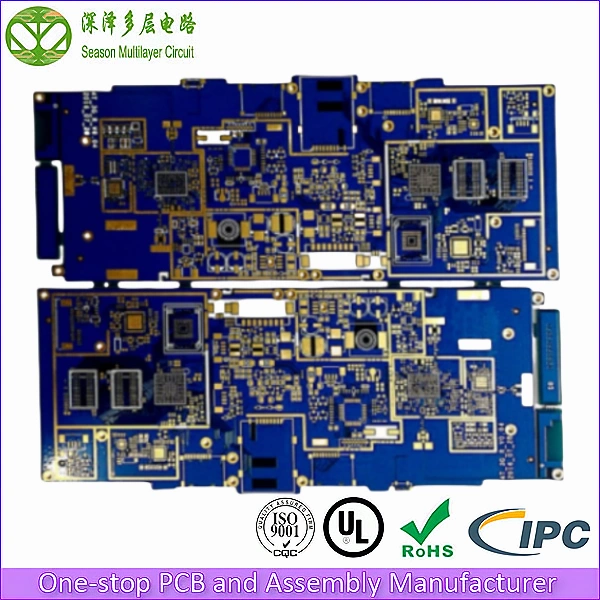
4. Component Placement Strategies
- Linear alignment: Arrange high-power ICs in rows parallel to airflow.
- Spacing: Avoid clustering heat-generating parts to prevent hotspots.
5. Thermal Zoning Based on Heat Tolerance
- Upstream (cooling inlet): Place sensitive components (sensors, ICs).
- Downstream (outlet): Position high-tolerance parts (power converters).
6. Peripheral Mounting for High-Wattage Devices
Mount power transistors, LEDs, or motor drivers near PCB edges to:
- Shorten heat paths to chassis/enclosure.
- Minimize thermal impact on central components.
7. Reducing PCB Thermal Resistance (Rθ)
Key approaches:
- TIM selection: Gel, phase-change materials, or graphite sheets.
- Heatsink design: Fin density, base thickness, and forced-air vs. natural convection.
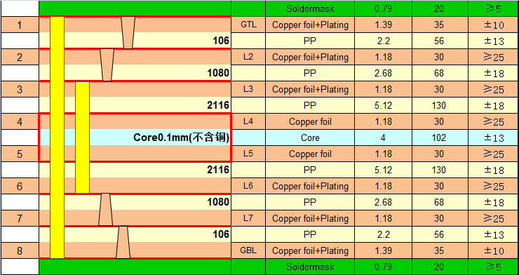
- Multilayer PCBs: Dedicated thermal layers (e.g., buried copper) lower Rθ.
Conclusion
Implementing these PCB thermal management techniques—from material selection to layout optimization—ensures stable operation, longevity, and compliance with industry standards like IPC-2221. For advanced PCB manufacturing support, consult Season MultiLayer Circuit for tailored solutions.
Pro Tip: Bookmark this guide for future reference! For deeper technical assistance, review our PCB fabrication capabilities or contact our engineering team.


