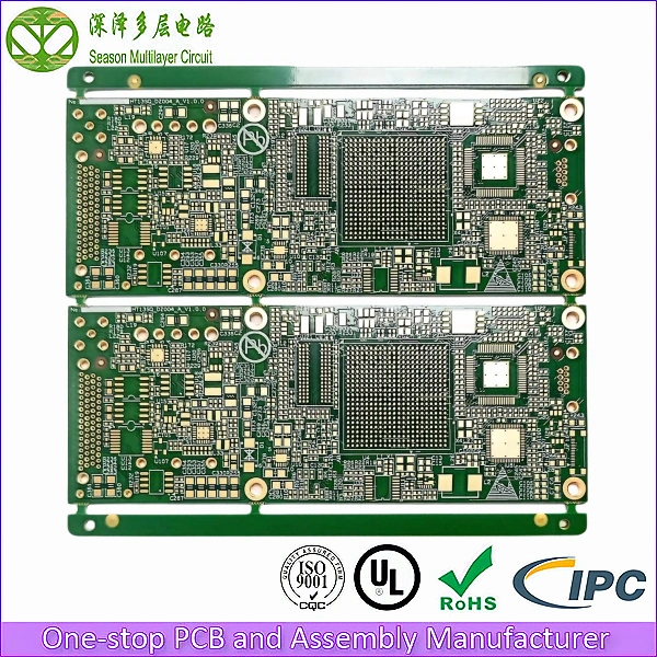
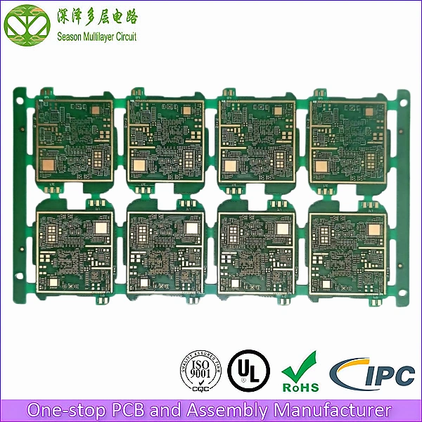
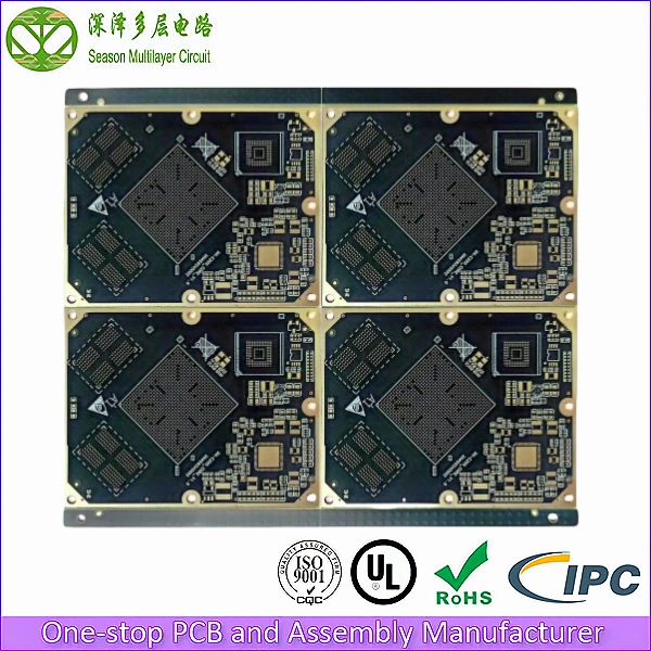
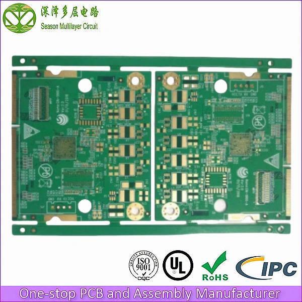
10-Layer 1-Step HDI Expedited Proofing
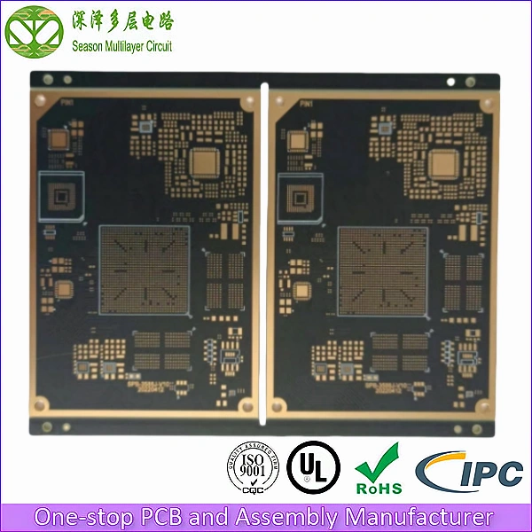
HDI Expedited Proofing
Layer Count: 10L(1+8+1)
Material: FR4 Tg170
Board Thickness: 1.0mm
Panel Size: 121.6*95mm/2
Outer Layer Copper Thickness: 1OZ
Inner Layer Copper Thickness: HOZ
Min Via Diameter: 0.20mm
Microvia Hole Size: 0.1mm
Trace Width/Spacing: 3/3mil
Min BGA Pad: 0.25mm
Surface Finish: ENIG1-2U’’
10-Layer 1-Step HDI Expedited Proofing,RK3588 core board, designed for industrial control applications.

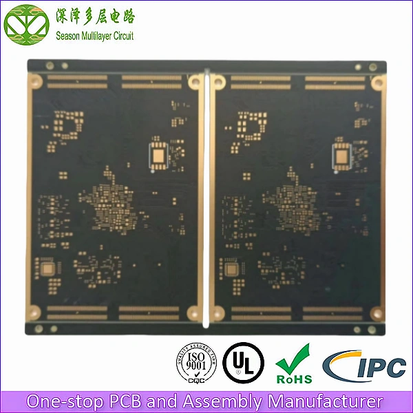
Accelerated Prototyping for High-Density Interconnect Solutions
In the fast-evolving electronics industry, rapid prototyping of High-Density Interconnect (HDI) boards has become a critical enabler for innovation. These advanced circuit boards, renowned for their ultra-compact design, exceptional reliability, and high integration, power cutting-edge applications ranging from smartphones and automotive systems to aerospace technologies. The demand for accelerated HDI prototyping services reflects the growing need to shorten product development cycles while maintaining rigorous quality standards.
Ⅰ.Advantages of HDI Expedited proofing
The urgency to deliver functional prototypes for time-sensitive projects has driven the evolution of specialized prototyping methodologies. Key benefits include:
- Precision Engineering Under Time Constraints
Despite compressed timelines, accelerated HDI solutions prioritize technical excellence. Advanced substrates like ultra-low-loss laminates (Dk ≤ 3.5 at 10 GHz) and laser-drilled microvias (≤75μm diameter) ensure signal integrity in space-constrained designs. Statistical process controls maintain ±5% impedance tolerances even during expedited runs. - Optimized Production Cadence
Leading manufacturers achieve 5-7 day turnaround times for 8-layer HDI prototypes through parallelized workflows. Automated laser direct imaging (LDI) systems enable 50μm line/space resolution, while plasma desmear technology guarantees uniform via preparation for complex stacked microvia architectures. - Application-Specific Customization
Prototyping services accommodate diverse requirements:- Mixed-signal layouts with embedded passive components
- Hybrid rigid-flex configurations for wearable devices
- High-speed designs supporting PCIe 5.0 (32 GT/s) and DDR5 interfaces
- Lifecycle Cost Efficiency
While accelerated prototyping incurs 25-40% higher initial costs compared to standard services, it reduces overall development expenses by 30% through early design validation. Advanced simulation tools minimize iterative revisions, with 92% of prototypes requiring ≤2 design iterations.
Ⅱ.Technical Workflow for Time-Critical Prototypes
The production of high-reliability HDI prototypes follows an optimized sequence:
Phase 1: Design Preparation
- Signal Integrity Modeling: 3D electromagnetic simulations for crosstalk mitigation
- Thermal Analysis: Finite element modeling to predict thermal hotspots
- Stackup Optimization: 10-layer 2+N+2 configurations with buried capacitance layers
Phase 2: Advanced Fabrication
- Laser Drilling: CO₂/UV hybrid systems create 75μm microvias with 1:1 aspect ratios
- Pattern Plating: Pulse-reverse plating achieves 18μm copper uniformity
- Surface Finishing: ENEPIG (Electroless Nickel Electroless Palladium Immersion Gold) for 0.15μm Au thickness
Phase 3: Quality Assurance
- Automated optical inspection (AOI) with 5μm defect detection
- Time-domain reflectometry (TDR) for impedance profile verification
- Thermal cycling tests (-55°C to +125°C, 500 cycles)
Ⅲ.Critical Success Parameters
To ensure prototype reliability, manufacturers must address:
| Parameter | Target Specification | Measurement Method |
|---|---|---|
| Dielectric Thickness | ±3% variation | Laser micrometer |
| Copper Roughness (Rz) | ≤3.5μm | Atomic force microscopy |
| Hole Wall Angularity | ≤5° deviation | Cross-sectional analysis |
| Registration Accuracy | ±15μm layer-to-layer | X-ray inspection |
Ⅳ.Season Multilayer Circuits: Pioneering HDI Expedited Proofing Solutions
With 11 years of expertise in complex HDI manufacturing, Season Multilayer Circuit delivers:
- 10-layer 1-step HDI prototypes within 168 hours
- First-pass success rate exceeding 98.5% for impedance-critical designs
- Custom material integration including Rogers 4350B and Megtron 6
Current pricing for expedited services reflects intensive R&D investments in:
- AI-powered design rule checks
- Robotic process automation cells
- In-house material characterization labs
Industry analysts project 18-22% cost reductions by 2026 as machine learning algorithms optimize material utilization and cycle times.
Ⅴ.Strategic Implementation Guidelines
- Design File Preparation: Submit IPC-2581B files with annotated impedance requirements
- Material Selection: Specify glass transition temperature (Tg ≥ 170°C) for high-T applications
- Testing Protocols: Implement boundary scan testing for complex BGAs
By leveraging HDI Expedited Proofing, engineering teams can achieve:
- 40% faster time-to-market for 5G infrastructure components
- 60% reduction in signal loss for millimeter-wave applications
- 35% improvement in thermal management for automotive ECUs
This strategic approach enables companies to balance urgent project timelines with uncompromised technical performance, ultimately driving innovation in next-generation electronics.


