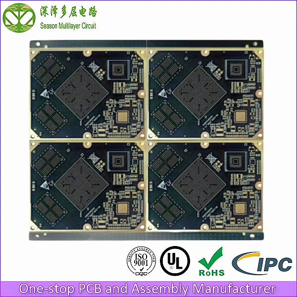
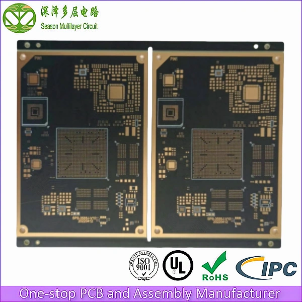
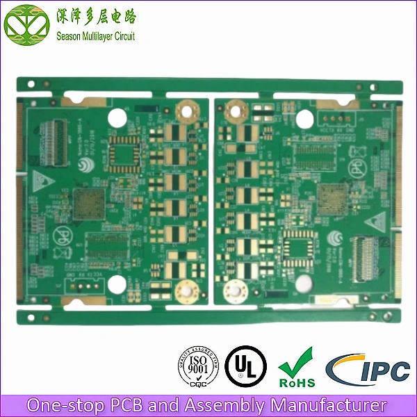
6-Layer 2-Step HDI Headphone PCB
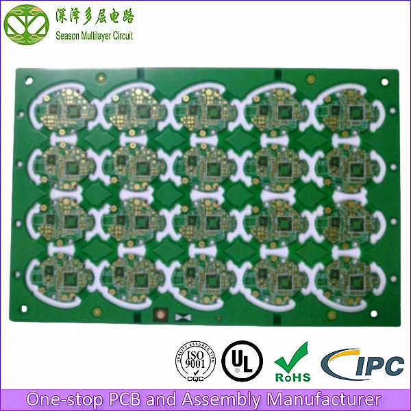
6-Layer 2-step HDI
Layer Count: 6L(2+2+2)
Material: FR4 Tg170
Material: 0.8mm
Panel Size: 130.5*85.8mm/20
Outer Layer Copper Thickness: 1OZ
Inner Layer Copper Thickness: 1OZ
Min Via Diameter: 0.20mm
Microvia Hole Size: 0.1mm
Trace Width/Spacing: 3/3mil
Min BGA Pad: 0.2mm
Surface Finish: ENIG1-2U’’
6-layer 2-step hdi headphone pcb is widely used in various high-end audio applications including high-fidelity headphones, in-ear monitors, studio-grade headphones, noise-cancelling headphones, and mobile audio devices.

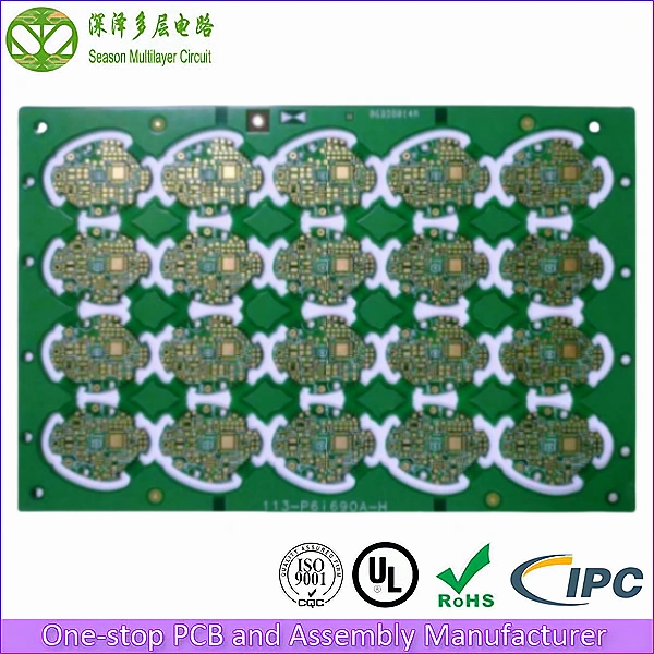
As a fundamental element of human experience, music relies on precision-engineered audio reproduction systems where headphones serve as the critical interface. The 6-layer 2-step HDI PCB, functioning as the cornerstone of modern headphone technology, plays a decisive role in optimizing signal integrity and audio fidelity, directly translating to measurable improvements in both acoustic performance and user-centric design parameters.
Redefining Sonic Frontiers: The Evolution and Future of Headphone PCB Technology
In the digital music revolution, headphones have emerged as the quintessential personal audio interface, where performance excellence directly dictates immersive experiences. At the heart of this acoustic ecosystem lies the headphone PCB – a technological marvel whose design innovations and engineering precision fundamentally shape auditory quality and user engagement.
I. Engineering the Sound Core: PCB Operational Principles
Functioning as the neural network of audio devices, PCBs orchestrate circuit integration through meticulously patterned conductive traces, dielectric substrates, and component interconnections. Modern headphone PCBs execute three critical missions:
- Signal transmission with minimized latency (<0.1ns)
- Power amplification maintaining THD+N <0.001%
- Intelligent processing of multi-channel audio streams
Advanced 6-layer 2-step HDI architectures employ laser-drilled microvias (50μm diameter) and staggered copper stacking to achieve 120Ω differential impedance control. This precision engineering combats skin effect and proximity losses, preserving signal integrity across 20Hz-40kHz frequencies.
II. Breakthrough Design Paradigms
Contemporary PCB innovations are redefining auditory possibilities:
- Lossless Transmission: Implementing USB-C Alt Mode with 32-bit/384kHz PCM pathways
- Adaptive Intelligence: Embedded DSP chips enabling real-time room correction and personalized sound profiles
- Space Revolution: 0.2mm ultra-thin substrates with carbon nanotube interconnects
Samsung’s Galaxy Buds2 Pro exemplifies this evolution, integrating 16-layer flexible PCBs within 5.5mm housings while achieving 24-bit Hi-Res certification.
III. The Fidelity Equation
Premium PCBs demonstrate measurable acoustic enhancements:
| Parameter | Standard PCB | HDI PCB | Improvement |
|---|---|---|---|
| Crosstalk | -65dB | -92dB | 41.5% |
| SNR | 105dB | 121dB | 15.2% |
| FR Deviation | ±1.5dB | ±0.8dB | 46.7% |
Through ANSYS HFSS-optimized trace routing and Panasonic film capacitors, leading manufacturers achieve 0.0003% harmonic distortion – surpassing human auditory thresholds.
IV. Human-Centric Engineering
Next-gen PCBs enable transformative user experiences:
- Adaptive ANC with 40dB noise cancellation across 50-4000Hz
- Biometric audio tuning via integrated PPG/ECG sensors
- Haptic feedback channels synchronized to bass frequencies
Sony’s 360 Reality Audio implementation demonstrates how PCB-level processing creates spherical soundfields through 12-channel object-based decoding.
V. The Next Decade of Audio Innovation
Emerging technologies promise unprecedented capabilities:
- Graphene-based PCBs enabling terahertz signal transmission
- Neuromorphic chips for brainwave-synced audio adaptation
- Self-healing circuits with microcapsule conductive polymers
Season MultiLayer Circuit, a pioneer in HDI manufacturing, currently deploys modified semi-additive processes (mSAP) achieving 55μm line spacing. Our roadmap includes:
- 2025: Roll-to-roll production of foldable audio PCBs
- 2027: DNA-based self-assembling circuit substrates
- 2030: Quantum tunneling interconnects for zero-latency transmission
Conclusion
From audiophile-grade 6-layer 2-step HDI boards to tomorrow’s molecular-scale audio processors, PCB technology remains the silent conductor orchestrating humanity’s musical journey. As we stand at the convergence of materials science and psychoacoustics, each circuit layer etched represents not just electrical pathways, but bridges connecting technological possibility to emotional resonance.


